R5F21217JFP#U1 Renesas Electronics America, R5F21217JFP#U1 Datasheet - Page 495
R5F21217JFP#U1
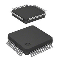
Manufacturer Part Number
R5F21217JFP#U1
Description
MCU FLASH 48K 2.5K CMOS 48LQFP
Manufacturer
Renesas Electronics America
Series
R8C/2x/21r
Datasheet
1.R5F21216JFP.pdf
(503 pages)
Specifications of R5F21217JFP#U1
Core Processor
R8C
Core Size
16/32-Bit
Speed
20MHz
Connectivity
I²C, LIN, SIO, SSU, UART/USART
Peripherals
POR, Voltage Detect, WDT
Number Of I /o
41
Program Memory Size
48KB (48K x 8)
Program Memory Type
FLASH
Ram Size
2.5K x 8
Voltage - Supply (vcc/vdd)
2.7 V ~ 5.5 V
Data Converters
A/D 12x10b
Oscillator Type
Internal
Operating Temperature
-40°C ~ 85°C
Package / Case
48-LQFP
Lead Free Status / RoHS Status
Lead free / RoHS Compliant
Eeprom Size
-
Available stocks
Company
Part Number
Manufacturer
Quantity
Price

Part Number:
R5F21217JFP#U1R5F21217JFP
Manufacturer:
Renesas Electronics America
Quantity:
10 000


Rev.
1.00
REVISION HISTORY
Nov 15, 2006
Date
Page
351
352
354
365
369
371
374
375
376
378
379
381
389
390
393
396
Figure 17.9 Example of Header Field Reception Flowchart (2);
“When the SBE bit in the LINCR register is 0(Unmasked after Synch Break is
detected), timer RA is usable in timer mode after the SBDCT flag in the LINST
register is set to 1.” added.
Figure 17.10 Example of Header Field Reception Flowchart (3);
“When the SBE bit in the LINCR register is 1 (Unmasked after Synch Field
measurement is completed), timer RA is usable in timer mode after the SFDCT
flag in the LINST register is set to 1.” added.
17.4.4 Hardware LIN End Processing and Figure 17.12 Example of Hardware
LIN Communication Completion Flowchart added.
Figure 18.6 ADCON0 Register in Repeat Mode, in the Function of Frequency
select bit 0;
Figure 18.10 Internal Equivalent Circuit of Analog Input;
18.7 Notes on A/D Converter, on the 5th line from the bottom;
19.2 Memory Map, on the 4th line from the bottom;
“When rewriting the block 2 and block 3 in CPU rewrite mode, set the FMR02 bit
in the FMR0 register to 1 (rewrite enables).” added.
Figure 19.1 Flash Memory Block Diagram for R8C/20 Group revised.
Figure 19.2 Flash Memory Block Diagram for R8C/21 Group revised.
Figure 19.4 OFS Register;
enabled after reset)” corrected.
Table 19.3 Differences between EW0 Mode and EW1 Mode;
19.4.2.3 FMR02 Bit;
not ~” corrected.
19.4.3.1 Read Array Command, on the bottom line;
19.4.3.2 Read Status Register Command, on the bottom line;
command is written.” added.
Figure 19.13 Program Command (When Suspend Function Enabled) revised.
NOTE3 added.
Figure 19.15 Block Erase Command (When Erase-Suspend Function Enabled)
revised.
NOTE3 added.
Figure 19.16 Full Status Check and Handling Procedure for Individual Errors;
“1: Select fOCO-F” → “Do not set” revised.
“i = 4” → “i = 12” corrected.
“Do not select the fOCO-F for the φAD.” added.
NOTE2; “LVD0ON” → “LVD1ON” and
“(voltage monitor 0 reset enabled after reset)” → “voltage monitor 0 reset
Modes After Read Status Register added.
“The block 1 and block 0 do not ~” → “The block0 block1 block2, and block3 do
“In addition, the MCU enters read array mode after a reset.” added.
“The MCU remains in read status register mode until the next read array
“FMR07 = 0?” → “FMR07 = 1?” and
“FMR06 = 0?” → “FMR06 = 1?” corrected.
R8C/20 Group, R8C/21 Group Hardware Manual
C - 19
Description
Summary
Related parts for R5F21217JFP#U1
Image
Part Number
Description
Manufacturer
Datasheet
Request
R

Part Number:
Description:
KIT STARTER FOR M16C/29
Manufacturer:
Renesas Electronics America
Datasheet:

Part Number:
Description:
KIT STARTER FOR R8C/2D
Manufacturer:
Renesas Electronics America
Datasheet:

Part Number:
Description:
R0K33062P STARTER KIT
Manufacturer:
Renesas Electronics America
Datasheet:

Part Number:
Description:
KIT STARTER FOR R8C/23 E8A
Manufacturer:
Renesas Electronics America
Datasheet:

Part Number:
Description:
KIT STARTER FOR R8C/25
Manufacturer:
Renesas Electronics America
Datasheet:

Part Number:
Description:
KIT STARTER H8S2456 SHARPE DSPLY
Manufacturer:
Renesas Electronics America
Datasheet:

Part Number:
Description:
KIT STARTER FOR R8C38C
Manufacturer:
Renesas Electronics America
Datasheet:

Part Number:
Description:
KIT STARTER FOR R8C35C
Manufacturer:
Renesas Electronics America
Datasheet:

Part Number:
Description:
KIT STARTER FOR R8CL3AC+LCD APPS
Manufacturer:
Renesas Electronics America
Datasheet:
Part Number:
Description:
KIT STARTER FOR RX610
Manufacturer:
Renesas Electronics America
Datasheet:

Part Number:
Description:
KIT STARTER FOR R32C/118
Manufacturer:
Renesas Electronics America
Datasheet:

Part Number:
Description:
KIT DEV RSK-R8C/26-29
Manufacturer:
Renesas Electronics America
Datasheet:

Part Number:
Description:
KIT STARTER FOR SH7124
Manufacturer:
Renesas Electronics America
Datasheet:

Part Number:
Description:
KIT STARTER FOR H8SX/1622
Manufacturer:
Renesas Electronics America
Datasheet:

Part Number:
Description:
KIT DEV FOR SH7203
Manufacturer:
Renesas Electronics America
Datasheet: