R5F21217JFP#U1 Renesas Electronics America, R5F21217JFP#U1 Datasheet - Page 303
R5F21217JFP#U1
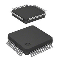
Manufacturer Part Number
R5F21217JFP#U1
Description
MCU FLASH 48K 2.5K CMOS 48LQFP
Manufacturer
Renesas Electronics America
Series
R8C/2x/21r
Datasheet
1.R5F21216JFP.pdf
(503 pages)
Specifications of R5F21217JFP#U1
Core Processor
R8C
Core Size
16/32-Bit
Speed
20MHz
Connectivity
I²C, LIN, SIO, SSU, UART/USART
Peripherals
POR, Voltage Detect, WDT
Number Of I /o
41
Program Memory Size
48KB (48K x 8)
Program Memory Type
FLASH
Ram Size
2.5K x 8
Voltage - Supply (vcc/vdd)
2.7 V ~ 5.5 V
Data Converters
A/D 12x10b
Oscillator Type
Internal
Operating Temperature
-40°C ~ 85°C
Package / Case
48-LQFP
Lead Free Status / RoHS Status
Lead free / RoHS Compliant
Eeprom Size
-
Available stocks
Company
Part Number
Manufacturer
Quantity
Price

Part Number:
R5F21217JFP#U1R5F21217JFP
Manufacturer:
Renesas Electronics America
Quantity:
10 000


R8C/20 Group, R8C/21 Group
Rev.2.00 Aug 27, 2008
REJ09B0250-0200
Figure 16.2
SS Control Register H
b7 b6 b5 b4 b3 b2 b1 b0
NOTES:
1.
2.
3.
The set clock is used w hen the internal clock is selected.
The SSCK pin functions as the transfer clock output pin w hen the MSS bit is set to 1 (operates as master device).
The MSS bit is set to 0 (operates as slave device) w hen the CE bit in the SSSR register is set to 1 (conflict error
occurs).
The RSSTP bit is disabled w hen the MSS bit is set to 0 (operates as slave device).
SSCRH Register
Bit Symbol
(b4-b3)
Symbol
SSCRH
RSSTP
CKS0
CKS1
CKS2
Page 285 of 458
MSS
(b7)
—
—
Transfer clock rate select bit
Nothing is assigned. If necessary, set to 0.
When read, the content is 0.
Master/slave device select bit
Receive single stop bit
Nothing is assigned. If necessary, set to 0.
When read, the content is 0.
Address
Bit Name
00B8h
(3)
(1)
(2)
b2 b1 b0
0 0 0 : f1/256
0 0 1 : f1/128
0 1 0 : f1/64
0 1 1 : f1/32
1 0 0 : f1/16
1 0 1 : f1/8
1 1 0 : f1/4
1 1 1 : Do not set
0 : Operates as slave device
1 : Operates as master device
0 : Maintains receive operation after
1 : Completes receive operation after
receiving 1-byte data
receiving 1-byte data
16. Clock Synchronous Serial Interface
After Reset
Function
00h
RW
RW
RW
RW
RW
RW
—
—
Related parts for R5F21217JFP#U1
Image
Part Number
Description
Manufacturer
Datasheet
Request
R

Part Number:
Description:
KIT STARTER FOR M16C/29
Manufacturer:
Renesas Electronics America
Datasheet:

Part Number:
Description:
KIT STARTER FOR R8C/2D
Manufacturer:
Renesas Electronics America
Datasheet:

Part Number:
Description:
R0K33062P STARTER KIT
Manufacturer:
Renesas Electronics America
Datasheet:

Part Number:
Description:
KIT STARTER FOR R8C/23 E8A
Manufacturer:
Renesas Electronics America
Datasheet:

Part Number:
Description:
KIT STARTER FOR R8C/25
Manufacturer:
Renesas Electronics America
Datasheet:

Part Number:
Description:
KIT STARTER H8S2456 SHARPE DSPLY
Manufacturer:
Renesas Electronics America
Datasheet:

Part Number:
Description:
KIT STARTER FOR R8C38C
Manufacturer:
Renesas Electronics America
Datasheet:

Part Number:
Description:
KIT STARTER FOR R8C35C
Manufacturer:
Renesas Electronics America
Datasheet:

Part Number:
Description:
KIT STARTER FOR R8CL3AC+LCD APPS
Manufacturer:
Renesas Electronics America
Datasheet:
Part Number:
Description:
KIT STARTER FOR RX610
Manufacturer:
Renesas Electronics America
Datasheet:

Part Number:
Description:
KIT STARTER FOR R32C/118
Manufacturer:
Renesas Electronics America
Datasheet:

Part Number:
Description:
KIT DEV RSK-R8C/26-29
Manufacturer:
Renesas Electronics America
Datasheet:

Part Number:
Description:
KIT STARTER FOR SH7124
Manufacturer:
Renesas Electronics America
Datasheet:

Part Number:
Description:
KIT STARTER FOR H8SX/1622
Manufacturer:
Renesas Electronics America
Datasheet:

Part Number:
Description:
KIT DEV FOR SH7203
Manufacturer:
Renesas Electronics America
Datasheet: