R5F21217JFP#U1 Renesas Electronics America, R5F21217JFP#U1 Datasheet - Page 487
R5F21217JFP#U1
Manufacturer Part Number
R5F21217JFP#U1
Description
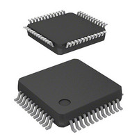
MCU FLASH 48K 2.5K CMOS 48LQFP
Manufacturer
Renesas Electronics America
Series
R8C/2x/21r
Datasheet
1.R5F21216JFP.pdf
(503 pages)
Specifications of R5F21217JFP#U1
Core Processor
R8C
Core Size
16/32-Bit
Speed
20MHz
Connectivity
I²C, LIN, SIO, SSU, UART/USART
Peripherals
POR, Voltage Detect, WDT
Number Of I /o
41
Program Memory Size
48KB (48K x 8)
Program Memory Type
FLASH
Ram Size
2.5K x 8
Voltage - Supply (vcc/vdd)
2.7 V ~ 5.5 V
Data Converters
A/D 12x10b
Oscillator Type
Internal
Operating Temperature
-40°C ~ 85°C
Package / Case
48-LQFP
Lead Free Status / RoHS Status
Lead free / RoHS Compliant
Eeprom Size
-
Available stocks
Company
Part Number
Manufacturer
Quantity
Price

Part Number:
R5F21217JFP#U1R5F21217JFP
Manufacturer:
Renesas Electronics America
Quantity:
10 000


Rev.
0.20
REVISION HISTORY
Jun 28, 2006
Date
404 to 423 20. Electrical Characteristics revised.
Page
377
379
380
381
382
384
385
389
390
391
392
393
396
398
399
401
Figure 19.4 OFS Register revised.
19.4.2 EW1 Mode, on the 3rd line;
19.4.2.1 FMR00 Bit, on the 1st line;
19.4.2.16 FMR47 Bit revised.
Figure 19.5 FMR0 Register;
Figure 19.7 FMR4 Register;
Figure 19.8 Timing of Suspend Operation revised.
19.4.3.4 Program Command, on the 5th line;
Figure 19.13 Program Command (When Suspend Function Enabled)
added.
19.4.3.5 Block Erase, on the 11th line;
Figure 19.15 Block Erase Command (When Erase-Suspend Function
Enabled) revised.
Table 19.5 Status Register Bits, Value after Reset of SR7 (D7)
19.5 Standard Serial I/O Mode, on the 3rd line;
Table 19.7 Pin Functions (Flash Memory Standard Serial I/O Mode 2)
revised.
Figure 19.17 Pin Connections for Standard Serial I/O Mode 3;
Figure 19.18 Pin Processing in Standard Serial I/O Mode 2 added.
Figure 19.19 Pin Processing in Standard Serial I/O Mode 3;
19.7 Notes on Flash Memory;
R8C/20 Group, R8C/21 Group Hardware Manual
“Do not execute software command ~” → “Do not execute command
~” revised.
“(including suspend periods)” added.
NOTE6 added.
NOTES revised.
“The FMR00 bit is ~ completes.” → “When suspend function ~ auto-
programming completes.” revised.
“The block erase ~ program suspend.” → “Do not use ~ program-
suspend” revised.
“0” → “1” corrected.
“Standard serial I/O ~ interface” → “There are three ~ serial I/O mode
3.” revised.
“Figure 19.17 Pin Connections for Standard Serial I/O Mode” →
“Figure 19.17 Pin Connections for Standard Serial I/O Mode 3”
revised.
“Figure 19.19 Pin Processing in Standard Serial I/O Mode” → “Figure
19.19 Pin Processing in Standard Serial I/O Mode 3” revised.
“19.7 Precautions on Flash Memory Version” → “19.7 Notes on Flash
Memory” revised.
C - 11
Description
Summary
Related parts for R5F21217JFP#U1
Image
Part Number
Description
Manufacturer
Datasheet
Request
R

Part Number:
Description:
KIT STARTER FOR M16C/29
Manufacturer:
Renesas Electronics America
Datasheet:

Part Number:
Description:
KIT STARTER FOR R8C/2D
Manufacturer:
Renesas Electronics America
Datasheet:

Part Number:
Description:
R0K33062P STARTER KIT
Manufacturer:
Renesas Electronics America
Datasheet:

Part Number:
Description:
KIT STARTER FOR R8C/23 E8A
Manufacturer:
Renesas Electronics America
Datasheet:

Part Number:
Description:
KIT STARTER FOR R8C/25
Manufacturer:
Renesas Electronics America
Datasheet:

Part Number:
Description:
KIT STARTER H8S2456 SHARPE DSPLY
Manufacturer:
Renesas Electronics America
Datasheet:

Part Number:
Description:
KIT STARTER FOR R8C38C
Manufacturer:
Renesas Electronics America
Datasheet:

Part Number:
Description:
KIT STARTER FOR R8C35C
Manufacturer:
Renesas Electronics America
Datasheet:

Part Number:
Description:
KIT STARTER FOR R8CL3AC+LCD APPS
Manufacturer:
Renesas Electronics America
Datasheet:
Part Number:
Description:
KIT STARTER FOR RX610
Manufacturer:
Renesas Electronics America
Datasheet:

Part Number:
Description:
KIT STARTER FOR R32C/118
Manufacturer:
Renesas Electronics America
Datasheet:

Part Number:
Description:
KIT DEV RSK-R8C/26-29
Manufacturer:
Renesas Electronics America
Datasheet:

Part Number:
Description:
KIT STARTER FOR SH7124
Manufacturer:
Renesas Electronics America
Datasheet:

Part Number:
Description:
KIT STARTER FOR H8SX/1622
Manufacturer:
Renesas Electronics America
Datasheet:

Part Number:
Description:
KIT DEV FOR SH7203
Manufacturer:
Renesas Electronics America
Datasheet: