R5F21217JFP#U1 Renesas Electronics America, R5F21217JFP#U1 Datasheet - Page 155
R5F21217JFP#U1
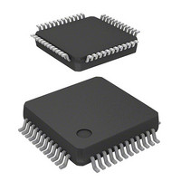
Manufacturer Part Number
R5F21217JFP#U1
Description
MCU FLASH 48K 2.5K CMOS 48LQFP
Manufacturer
Renesas Electronics America
Series
R8C/2x/21r
Datasheet
1.R5F21216JFP.pdf
(503 pages)
Specifications of R5F21217JFP#U1
Core Processor
R8C
Core Size
16/32-Bit
Speed
20MHz
Connectivity
I²C, LIN, SIO, SSU, UART/USART
Peripherals
POR, Voltage Detect, WDT
Number Of I /o
41
Program Memory Size
48KB (48K x 8)
Program Memory Type
FLASH
Ram Size
2.5K x 8
Voltage - Supply (vcc/vdd)
2.7 V ~ 5.5 V
Data Converters
A/D 12x10b
Oscillator Type
Internal
Operating Temperature
-40°C ~ 85°C
Package / Case
48-LQFP
Lead Free Status / RoHS Status
Lead free / RoHS Compliant
Eeprom Size
-
Available stocks
Company
Part Number
Manufacturer
Quantity
Price

Part Number:
R5F21217JFP#U1R5F21217JFP
Manufacturer:
Renesas Electronics America
Quantity:
10 000


R8C/20 Group, R8C/21 Group
Rev.2.00 Aug 27, 2008
REJ09B0250-0200
14.2
Figure 14.13
Timer RB is an 8-bit timer with an 8-bit prescaler.
The prescaler and timer consist of the reload register and counter. (Refer to Table 14.7 to 14.10 the Specification
of Each Modes).
Timer RB contains the timer RB primary and timer RB secondary as the reload register.
The count source for timer RB is the operating clock that regulates the timing of timer operations such as counting
and reloading.
Figure 14.13 shows the Block Diagram of Timer RB. Figures 14.14 and 14.16 show the registers associated with
timer RB.
Timer RB contains four operation modes listed as follows:
Timer RA underflow
TRBO pin
INT0 pin
TSTART, TCSTF: TRBCR register
TOSST: TRBOCR register
TOPL, TOCNT, INOSTG, INOSEG: TRBIOC register
TMOD1 to TMOD0, TCK1 to TCK0, TCKCUT: TRBMR register
•
•
•
•
TCK1 to TCK0 bit
Timer mode:
Programmable waveform generation mode:
Programmable one-shot generation mode:
Programmable wait one-shot generation mode: The timer outputs delayed one-shot pulse.
Timer RB
f1
f2
TMOD1 to TMOD0 bit
= 01b
f8
Block Diagram of Timer RB
= 00b
= 01b
= 10b
= 11b
,
10b, 11b
TCKCUT bit
Page 137 of 458
TOCNT = 1
TOCNT = 0
Digital filter
P3_1 bit in P3 register
edge or both edges
TRBPRE register
selected to be one
register
Reload
Input polarity
INT0EN bit
INT0PL bit
(Prescaler)
TSTART bit
Counter
The timer counts an internal count source (peripheral function
clock or timer RA underflows).
The timer outputs pulses of a given width successively.
The timer outputs one-shot pulse.
Peripheral data bus
TMOD1 to TMOD0 bit
= 10b or 11b
TOPL = 1
TOPL = 0
register
Reload
INOSEG bit
TRBSC
register
Polarity
Counter (timer RB)
select
(Timer)
Q
Q
Toggle flip-flop
TOSSTF bit
register
Reload
CLR
INOSTG bit
TRBPR
register
CK
TCSTF bit
TMOD1 to TMOD0 bit
= 01b
Timer RB interrupt
INT0 interrupt
,
10b, 11b
14. Timers
Related parts for R5F21217JFP#U1
Image
Part Number
Description
Manufacturer
Datasheet
Request
R

Part Number:
Description:
KIT STARTER FOR M16C/29
Manufacturer:
Renesas Electronics America
Datasheet:

Part Number:
Description:
KIT STARTER FOR R8C/2D
Manufacturer:
Renesas Electronics America
Datasheet:

Part Number:
Description:
R0K33062P STARTER KIT
Manufacturer:
Renesas Electronics America
Datasheet:

Part Number:
Description:
KIT STARTER FOR R8C/23 E8A
Manufacturer:
Renesas Electronics America
Datasheet:

Part Number:
Description:
KIT STARTER FOR R8C/25
Manufacturer:
Renesas Electronics America
Datasheet:

Part Number:
Description:
KIT STARTER H8S2456 SHARPE DSPLY
Manufacturer:
Renesas Electronics America
Datasheet:

Part Number:
Description:
KIT STARTER FOR R8C38C
Manufacturer:
Renesas Electronics America
Datasheet:

Part Number:
Description:
KIT STARTER FOR R8C35C
Manufacturer:
Renesas Electronics America
Datasheet:

Part Number:
Description:
KIT STARTER FOR R8CL3AC+LCD APPS
Manufacturer:
Renesas Electronics America
Datasheet:
Part Number:
Description:
KIT STARTER FOR RX610
Manufacturer:
Renesas Electronics America
Datasheet:

Part Number:
Description:
KIT STARTER FOR R32C/118
Manufacturer:
Renesas Electronics America
Datasheet:

Part Number:
Description:
KIT DEV RSK-R8C/26-29
Manufacturer:
Renesas Electronics America
Datasheet:

Part Number:
Description:
KIT STARTER FOR SH7124
Manufacturer:
Renesas Electronics America
Datasheet:

Part Number:
Description:
KIT STARTER FOR H8SX/1622
Manufacturer:
Renesas Electronics America
Datasheet:

Part Number:
Description:
KIT DEV FOR SH7203
Manufacturer:
Renesas Electronics America
Datasheet: