HD64F36912GFH Renesas Electronics America, HD64F36912GFH Datasheet - Page 217
HD64F36912GFH
Manufacturer Part Number
HD64F36912GFH
Description
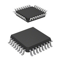
IC H8 MCU FLASH 8K 32-QFP
Manufacturer
Renesas Electronics America
Series
H8® H8/300H Tinyr
Datasheet
1.DF36912GFHV.pdf
(442 pages)
Specifications of HD64F36912GFH
Core Processor
H8/300H
Core Size
16-Bit
Speed
12MHz
Connectivity
I²C, SCI
Peripherals
LVD, POR, PWM, WDT
Number Of I /o
18
Program Memory Size
8KB (8K x 8)
Program Memory Type
FLASH
Ram Size
1.5K x 8
Voltage - Supply (vcc/vdd)
3 V ~ 5.5 V
Data Converters
A/D 4x10b
Oscillator Type
Internal
Operating Temperature
-20°C ~ 75°C
Package / Case
32-LQFP
Lead Free Status / RoHS Status
Contains lead / RoHS non-compliant
Eeprom Size
-
Available stocks
Company
Part Number
Manufacturer
Quantity
Price
Company:

Part Number:
HD64F36912GFH
Manufacturer:
Renesas Electronics America
Quantity:
10 000


12.6
The following types of contention or operation can occur in timer W operation.
1. The pulse width of the input clock signal and the input capture signal must be at least two
2. Writing to registers is performed in the T2 state of a TCNT write cycle.
3. Depending on the timing, TCNT may be incremented by a switch between different internal
4. If timer W enters module standby mode while an interrupt request is generated, the interrupt
5. The TOA to TOD bits in TCRW decide the value of the FTIO pin, which is output until the
system clock ( ) cycles; shorter pulses will not be detected correctly.
If counter clear signal occurs in the T2 state of a TCNT write cycle, clearing of the counter
takes priority and the write is not performed, as shown in figure 12.24. If counting-up is
generated in the TCNT write cycle to contend with the TCNT counting-up, writing takes
precedence.
clock sources. When TCNT is internally clocked, an increment pulse is generated from the
rising edge of an internal clock signal, that is divided system clock ( ). Therefore, as shown in
figure 12.25 the switch is from a low clock signal to a high clock signal, the switchover is seen
as a rising edge, causing TCNT to increment.
request cannot be cleared. Before entering module standby mode, disable interrupt requests.
first compare match occurs. Once a compare match occurs and this compare match changes the
values of FTIOA to FTIOD output, the values of the FTIOA to FTIOD pin output and the
values read from the TOA to TOD bits may differ. Moreover, when the writing to TCRW and
the generation of the compare match A to D occur at the same timing, the writing to TCRW
has the priority. Thus, output change due to the compare match is not reflected to the FTIOA
to FTIOD pins. Therefore, when bit manipulation instruction is used to write to TCRW, the
values of the FTIOA to FTIOD pin output may result in an unexpected result. When TCRW is
to be written to while compare match is operating, stop the counter once before accessing to
TCRW, read the port 8 state to reflect the values of FTIOA to FTIOD output, to TOA to TOD,
and then restart the counter. Figure 12.26 shows an example when the compare match and the
bit manipulation instruction to TCRW occur at the same timing.
Usage Notes
Rev. 3.00 Sep. 14, 2006 Page 187 of 408
Section 12 Timer W
REJ09B0105-0300
Related parts for HD64F36912GFH
Image
Part Number
Description
Manufacturer
Datasheet
Request
R


Part Number:
Description:
KIT STARTER FOR M16C/29
Manufacturer:
Renesas Electronics America
Datasheet:

Part Number:
Description:
KIT STARTER FOR R8C/2D
Manufacturer:
Renesas Electronics America
Datasheet:

Part Number:
Description:
R0K33062P STARTER KIT
Manufacturer:
Renesas Electronics America
Datasheet:

Part Number:
Description:
KIT STARTER FOR R8C/23 E8A
Manufacturer:
Renesas Electronics America
Datasheet:

Part Number:
Description:
KIT STARTER FOR R8C/25
Manufacturer:
Renesas Electronics America
Datasheet:

Part Number:
Description:
KIT STARTER H8S2456 SHARPE DSPLY
Manufacturer:
Renesas Electronics America
Datasheet:

Part Number:
Description:
KIT STARTER FOR R8C38C
Manufacturer:
Renesas Electronics America
Datasheet:

Part Number:
Description:
KIT STARTER FOR R8C35C
Manufacturer:
Renesas Electronics America
Datasheet:

Part Number:
Description:
KIT STARTER FOR R8CL3AC+LCD APPS
Manufacturer:
Renesas Electronics America
Datasheet:
Part Number:
Description:
KIT STARTER FOR RX610
Manufacturer:
Renesas Electronics America
Datasheet:

Part Number:
Description:
KIT STARTER FOR R32C/118
Manufacturer:
Renesas Electronics America
Datasheet:

Part Number:
Description:
KIT DEV RSK-R8C/26-29
Manufacturer:
Renesas Electronics America
Datasheet:

Part Number:
Description:
KIT STARTER FOR SH7124
Manufacturer:
Renesas Electronics America
Datasheet:

Part Number:
Description:
KIT STARTER FOR H8SX/1622
Manufacturer:
Renesas Electronics America
Datasheet: