HD64F36912GFH Renesas Electronics America, HD64F36912GFH Datasheet - Page 147
HD64F36912GFH
Manufacturer Part Number
HD64F36912GFH
Description
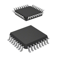
IC H8 MCU FLASH 8K 32-QFP
Manufacturer
Renesas Electronics America
Series
H8® H8/300H Tinyr
Datasheet
1.DF36912GFHV.pdf
(442 pages)
Specifications of HD64F36912GFH
Core Processor
H8/300H
Core Size
16-Bit
Speed
12MHz
Connectivity
I²C, SCI
Peripherals
LVD, POR, PWM, WDT
Number Of I /o
18
Program Memory Size
8KB (8K x 8)
Program Memory Type
FLASH
Ram Size
1.5K x 8
Voltage - Supply (vcc/vdd)
3 V ~ 5.5 V
Data Converters
A/D 4x10b
Oscillator Type
Internal
Operating Temperature
-20°C ~ 75°C
Package / Case
32-LQFP
Lead Free Status / RoHS Status
Contains lead / RoHS non-compliant
Eeprom Size
-
Available stocks
Company
Part Number
Manufacturer
Quantity
Price
Company:

Part Number:
HD64F36912GFH
Manufacturer:
Renesas Electronics America
Quantity:
10 000


The LSI of the H8/36912 Group and H8/36902 Group has 18 general I/O ports. Port 8 (P84 to
P80) is a large current port, which can drive 20 mA (@V
output. Any of these ports can become an input port immediately after a reset. They can also be
used as I/O pins of the on-chip peripheral modules or external interrupt input pins, and these
functions can be switched depending on the register settings. The registers for selecting these
functions can be divided into two types: those included in I/O ports and those included in each on-
chip peripheral module. General I/O ports are comprised of the port control register for controlling
inputs/outputs and the port data register for storing output data and can select inputs/outputs in bit
units. For functions in each port, see appendix B.1, I/O Port Block Diagrams. For the execution of
bit manipulation instructions to the port control register and port data register, see section 2.8.3,
Bit Manipulation Instruction.
9.1
Port 1 is a general I/O port also functioning as an IRQ interrupt input pin and timer V input pin.
Figure 9.1 shows its pin configuration.
Port 1 has the following registers.
Port mode register 1 (PMR1)
Port control register 1 (PCR1)
Port data register 1 (PDR1)
Port pull-up control register 1 (PUCR1)
Port 1
Figure 9.1 Port 1 Pin Configuration
Section 9 I/O Ports
Port 1
P17/IRQ3/TRGV
P14/IRQ0
OL
= 1.5 V) when a low level signal is
Rev. 3.00 Sep. 14, 2006 Page 117 of 408
Section 9 I/O Ports
REJ09B0105-0300
Related parts for HD64F36912GFH
Image
Part Number
Description
Manufacturer
Datasheet
Request
R


Part Number:
Description:
KIT STARTER FOR M16C/29
Manufacturer:
Renesas Electronics America
Datasheet:

Part Number:
Description:
KIT STARTER FOR R8C/2D
Manufacturer:
Renesas Electronics America
Datasheet:

Part Number:
Description:
R0K33062P STARTER KIT
Manufacturer:
Renesas Electronics America
Datasheet:

Part Number:
Description:
KIT STARTER FOR R8C/23 E8A
Manufacturer:
Renesas Electronics America
Datasheet:

Part Number:
Description:
KIT STARTER FOR R8C/25
Manufacturer:
Renesas Electronics America
Datasheet:

Part Number:
Description:
KIT STARTER H8S2456 SHARPE DSPLY
Manufacturer:
Renesas Electronics America
Datasheet:

Part Number:
Description:
KIT STARTER FOR R8C38C
Manufacturer:
Renesas Electronics America
Datasheet:

Part Number:
Description:
KIT STARTER FOR R8C35C
Manufacturer:
Renesas Electronics America
Datasheet:

Part Number:
Description:
KIT STARTER FOR R8CL3AC+LCD APPS
Manufacturer:
Renesas Electronics America
Datasheet:
Part Number:
Description:
KIT STARTER FOR RX610
Manufacturer:
Renesas Electronics America
Datasheet:

Part Number:
Description:
KIT STARTER FOR R32C/118
Manufacturer:
Renesas Electronics America
Datasheet:

Part Number:
Description:
KIT DEV RSK-R8C/26-29
Manufacturer:
Renesas Electronics America
Datasheet:

Part Number:
Description:
KIT STARTER FOR SH7124
Manufacturer:
Renesas Electronics America
Datasheet:

Part Number:
Description:
KIT STARTER FOR H8SX/1622
Manufacturer:
Renesas Electronics America
Datasheet: