MC9S08RG60CFGE Freescale Semiconductor, MC9S08RG60CFGE Datasheet - Page 13
MC9S08RG60CFGE
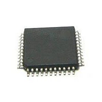
Manufacturer Part Number
MC9S08RG60CFGE
Description
IC MCU 60K FLASH 8MHZ 44LQFP
Manufacturer
Freescale Semiconductor
Series
HCS08r
Datasheet
1.MC9S08RE8FJE.pdf
(234 pages)
Specifications of MC9S08RG60CFGE
Core Processor
HCS08
Core Size
8-Bit
Speed
8MHz
Connectivity
SCI, SPI
Peripherals
LVD, POR, PWM, WDT
Number Of I /o
39
Program Memory Size
60KB (60K x 8)
Program Memory Type
FLASH
Ram Size
2K x 8
Voltage - Supply (vcc/vdd)
1.8 V ~ 3.6 V
Oscillator Type
Internal
Operating Temperature
-40°C ~ 85°C
Package / Case
44-LQFP
Processor Series
S08RG
Core
HCS08
Data Bus Width
8 bit
Data Ram Size
2 KB
Interface Type
SCI, SPI
Maximum Clock Frequency
8 MHz
Number Of Programmable I/os
39
Number Of Timers
2
Operating Supply Voltage
1.8 V to 3.6 V
Maximum Operating Temperature
+ 85 C
Mounting Style
SMD/SMT
3rd Party Development Tools
EWS08
Development Tools By Supplier
DEMO9S08RG60E
Minimum Operating Temperature
- 40 C
Controller Family/series
HCS08
No. Of I/o's
39
Ram Memory Size
60KB
Cpu Speed
8MHz
No. Of Timers
2
Embedded Interface Type
SCI, SPI
Rohs Compliant
Yes
For Use With
DEMO9S08RG60E - BOARD DEMO S08RG/RC/RD/RE FAMILY
Lead Free Status / RoHS Status
Lead free / RoHS Compliant
Eeprom Size
-
Data Converters
-
Lead Free Status / Rohs Status
Lead free / RoHS Compliant
Available stocks
Company
Part Number
Manufacturer
Quantity
Price
Company:

Part Number:
MC9S08RG60CFGE
Manufacturer:
Freescale Semiconductor
Quantity:
135
Company:
Part Number:
MC9S08RG60CFGE
Manufacturer:
Freescale Semiconductor
Quantity:
10 000


Section Number
13.4 SPI Registers and Control Bits ......................................................................................................171
14.1 Features .........................................................................................................................................180
14.2 Block Diagram ..............................................................................................................................180
14.3 Pin Description ..............................................................................................................................180
14.4 Functional Description ..................................................................................................................181
14.5 ACMP Status and Control Register (ACMP1SC) .........................................................................182
15.1 Introduction ...................................................................................................................................183
15.2 Background Debug Controller (BDC) ..........................................................................................184
15.3 On-Chip Debug System (DBG) ....................................................................................................192
15.4 Register Definition ........................................................................................................................196
Freescale Semiconductor
13.3.3
13.3.4
13.4.1
13.4.2
13.4.3
13.4.4
13.4.5
14.4.1
14.4.2
14.4.3
14.4.4
15.1.1
15.2.1
15.2.2
15.2.3
15.2.4
15.3.1
15.3.2
15.3.3
15.3.4
15.3.5
15.3.6
15.4.1
15.4.2
13.3.2.3 MISO1 — Master Data In, Slave Data Out ..................................................170
13.3.2.4 SS1 — Slave Select .......................................................................................170
SPI Interrupts ................................................................................................................171
Mode Fault Detection ...................................................................................................171
SPI Control Register 1 (SPI1C1) ..................................................................................172
SPI Control Register 2 (SPI1C2) ..................................................................................173
SPI Baud Rate Register (SPI1BR) ...............................................................................174
SPI Status Register (SPI1S) ..........................................................................................176
SPI Data Register (SPI1D) ...........................................................................................177
Interrupts .......................................................................................................................181
Wait Mode Operation ...................................................................................................181
Stop Mode Operation ...................................................................................................181
Background Mode Operation .......................................................................................181
Features .........................................................................................................................183
BKGD Pin Description .................................................................................................184
Communication Details ................................................................................................185
BDC Commands ...........................................................................................................189
BDC Hardware Breakpoint ..........................................................................................191
Comparators A and B ...................................................................................................192
Bus Capture Information and FIFO Operation .............................................................192
Change-of-Flow Information ........................................................................................193
Tag vs. Force Breakpoints and Triggers .......................................................................193
Trigger Modes ..............................................................................................................194
Hardware Breakpoints ..................................................................................................196
BDC Registers and Control Bits ...................................................................................196
15.4.1.1 BDC Status and Control Register (BDCSCR) ..............................................197
15.4.1.2 BDC Breakpoint Match Register (BDCBKPT) ............................................198
System Background Debug Force Reset Register (SBDFR) ........................................198
Analog Comparator (S08ACMPV1)
MC9S08RC/RD/RE/RG Data Sheet, Rev. 1.11
Development Support
Chapter 14
Chapter 15
Title
Page
13
Related parts for MC9S08RG60CFGE
Image
Part Number
Description
Manufacturer
Datasheet
Request
R

Part Number:
Description:
Manufacturer:
Freescale Semiconductor, Inc
Datasheet:
Part Number:
Description:
Manufacturer:
Freescale Semiconductor, Inc
Datasheet:
Part Number:
Description:
Manufacturer:
Freescale Semiconductor, Inc
Datasheet:
Part Number:
Description:
Manufacturer:
Freescale Semiconductor, Inc
Datasheet:
Part Number:
Description:
Manufacturer:
Freescale Semiconductor, Inc
Datasheet:
Part Number:
Description:
Manufacturer:
Freescale Semiconductor, Inc
Datasheet:
Part Number:
Description:
Manufacturer:
Freescale Semiconductor, Inc
Datasheet:
Part Number:
Description:
Manufacturer:
Freescale Semiconductor, Inc
Datasheet:
Part Number:
Description:
Manufacturer:
Freescale Semiconductor, Inc
Datasheet:
Part Number:
Description:
Manufacturer:
Freescale Semiconductor, Inc
Datasheet:
Part Number:
Description:
Manufacturer:
Freescale Semiconductor, Inc
Datasheet:
Part Number:
Description:
Manufacturer:
Freescale Semiconductor, Inc
Datasheet:
Part Number:
Description:
Manufacturer:
Freescale Semiconductor, Inc
Datasheet:
Part Number:
Description:
Manufacturer:
Freescale Semiconductor, Inc
Datasheet:
Part Number:
Description:
Manufacturer:
Freescale Semiconductor, Inc
Datasheet: