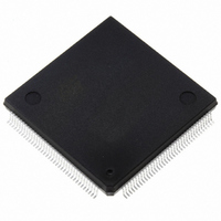
ST10F269Z2Q6 STMicroelectronics, ST10F269Z2Q6 Datasheet - Page 149

ST10F269Z2Q6
Manufacturer Part Number
ST10F269Z2Q6
Description
MCU 16BIT 256K FLASH 144PQFP
Manufacturer
STMicroelectronics
Series
ST10r
Specifications of ST10F269Z2Q6
Core Processor
ST10
Core Size
16-Bit
Speed
40MHz
Connectivity
CAN, EBI/EMI, SSC, UART/USART
Peripherals
POR, PWM, WDT
Number Of I /o
111
Program Memory Size
256KB (256K x 8)
Program Memory Type
FLASH
Ram Size
12K x 8
Voltage - Supply (vcc/vdd)
4.5 V ~ 5.5 V
Data Converters
A/D 16x10b
Oscillator Type
Internal
Operating Temperature
-40°C ~ 85°C
Package / Case
144-QFP
Controller Family/series
ST10
No. Of I/o's
111
Ram Memory Size
12KB
Cpu Speed
40MHz
No. Of Timers
5
Embedded Interface Type
CAN, SSC, USART
Rohs Compliant
Yes
Processor Series
ST10F26x
Core
ST10
Data Bus Width
16 bit
Data Ram Size
12 KB
Interface Type
CAN, SSC, USART
Maximum Clock Frequency
40 MHz
Number Of Programmable I/os
111
Number Of Timers
2 x 16 bit
Operating Supply Voltage
0.3 V to 4 V
Maximum Operating Temperature
+ 85 C
Mounting Style
SMD/SMT
Minimum Operating Temperature
- 40 C
On-chip Adc
16 bit x 10 bit
Lead Free Status / RoHS Status
Lead free / RoHS Compliant
Eeprom Size
-
Lead Free Status / Rohs Status
Details
Other names
497-4833
Available stocks
Company
Part Number
Manufacturer
Quantity
Price
Company:
Part Number:
ST10F269Z2Q6
Manufacturer:
ST
Quantity:
201
Company:
Part Number:
ST10F269Z2Q6
Manufacturer:
ST
Quantity:
745
Company:
Part Number:
ST10F269Z2Q6
Manufacturer:
STMicroelectronics
Quantity:
10 000
Part Number:
ST10F269Z2Q6
Manufacturer:
ST
Quantity:
20 000
ST10F269
21.4.4 - Prescaler Operation
When pins P0.15-13 (P0H.7-5) equal ’001’ during
reset, the CPU clock is derived from the internal
oscillator (input clock signal) by a 2:1 prescaler.
The frequency of f
f
duration of an individual TCL) is defined by the
period of the input clock f
The timings listed in the AC Characteristics that
refer to TCL therefore can be calculated using the
period of f
Note that if the bit OWDDIS in SYSCON register
is cleared, the PLL runs on its free-running
frequency and delivers the clock signal for the
Oscillator Watchdog. If bit OWDDIS is set, then
the PLL is switched off.
21.4.5 - Direct Drive
When pins P0.15-13 (P0H.7-5) equal ’011’ during
reset the on-chip phase locked loop is disabled
and the CPU clock is directly driven from the
internal oscillator with the input clock signal.
The frequency of f
frequency of f
(i.e. the duration of an individual TCL) is defined
by the duty cycle of the input clock f
Therefore, the timings given in this chapter refer to
the minimum TCL. This minimum value can be
calculated by the following formula:
For two consecutive TCLs, the deviation caused
by the duty cycle of f
duration of 2TCL is always 1/f
The minimum value TCL
once for timings that require an odd number of
TCLs (1,3,...). Timings that require an even
number of TCLs (2,4,...) may use the formula:
Note:
XTAL
and the high and low time of f
The address float timings in Multiplexed
bus mode (t
duration of TCL (TCL
DC
If the bit OWDDIS in SYSCON register is
cleared, the PLL runs on its free-running
frequency and delivers the clock signal for
the Oscillator Watchdog. If bit OWDDIS is
set, then the PLL is switched off.
TCL
XTAL
max
XTAL
min
DC
) instead of TCL
for any TCL.
2TCL
=
=
so the high and low time of f
CPU
11
1 f
duty cycle
XTAL
=
CPU
and t
XT
1 f XTAL
is half the frequency of
XTAL
min
is compensated, so the
A L
45
directly follows the
has to be used only
.
XTAL
l
) use the maximum
x
min
l
max
DC
.
.
XTAL
min
CPU
= 1/f
.
(i.e. the
XTAL
CPU
x
21.4.6 - Oscillator Watchdog (OWD)
An on-chip watchdog oscillator is implemented in
the ST10F269. This feature is used for safety
operation with external crystal oscillator (using
direct drive mode with or without prescaler). This
watchdog oscillator operates as following:
The reset default configuration enables the
watchdog oscillator. It can be disabled by setting
the OWDDIS (bit 4) of SYSCON register.
When the OWD is enabled, the PLL runs at its
free-running frequency, and it increments the
watchdog
frequency is between 2 and 10MHz. On each
transition of external clock, the watchdog counter
is cleared. If an external clock failure occurs, then
the watchdog counter overflows (after 16 PLL
clock cycles).
The CPU clock signal will be switched to the PLL
free-running clock signal, and the oscillator
watchdog Interrupt Request (XP3INT) is flagged.
The CPU clock will not switch back to the external
clock even if a valid external clock exits on XTAL1
pin. Only a hardware reset can switch the CPU
clock source back to direct clock input.
When the OWD is disabled, the CPU clock is
always external oscillator clock and the PLL is
switched off to decrease consumption supply
current.
21.4.7 - Phase Locked Loop
For all other combinations of pins P0.15-13
(P0H.7-5) during reset the on-chip phase locked
loop is enabled and it provides the CPU clock (see
Table 44 and Table 45). The PLL multiplies the
input frequency by the factor F which is selected
via the combination of pins P0.15-13 (f
x F). With every F’th transition of f
circuit synchronizes the CPU clock to the input
clock. This synchronization is done smoothly, so
the CPU clock frequency does not change
abruptly.
Due to this adaptation to the input clock the
frequency of f
locked to f
of f
individual TCLs.
The timings listed in the AC Characteristics that
refer to TCLs therefore must be calculated using
the minimum TCL that is possible under the
respective circumstances.
CPU
which also effects the duration of
XTAL
counter.
CPU
. The slight variation causes a jitter
is constantly adjusted so it is
The
PLL
XTAL
free-running
CPU
the PLL
149/184
= f
XTAL


