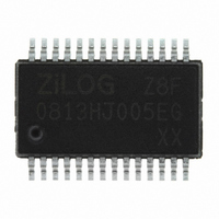
Z8F0813HJ005EG Zilog, Z8F0813HJ005EG Datasheet - Page 50

Z8F0813HJ005EG
Manufacturer Part Number
Z8F0813HJ005EG
Description
IC Z8 ENCORE MCU FLASH 8K 28SSOP
Manufacturer
Zilog
Series
Encore!® XP®r
Datasheet
1.Z8F0813PH005SC.pdf
(227 pages)
Specifications of Z8F0813HJ005EG
Core Processor
Z8
Core Size
8-Bit
Speed
5MHz
Connectivity
IrDA, UART/USART
Peripherals
Brown-out Detect/Reset, LED, POR, PWM, WDT
Number Of I /o
24
Program Memory Size
8KB (8K x 8)
Program Memory Type
FLASH
Ram Size
1K x 8
Voltage - Supply (vcc/vdd)
2.7 V ~ 3.6 V
Oscillator Type
Internal
Operating Temperature
-40°C ~ 105°C
Package / Case
28-SSOP
Lead Free Status / RoHS Status
Lead free / RoHS Compliant
Eeprom Size
-
Data Converters
-
Other names
269-4182
Z8F0813HJ005EG
Z8F0813HJ005EG
- Current page: 50 of 227
- Download datasheet (3Mb)
GPIO Alternate Functions
PS025203-0405
System
DATA
Clock
Bus
Data Register
Port Output
Many of the GPIO port pins can be used for general-purpose I/O and access to on-chip
peripheral functions such as the timers and serial communication devices. The Port A–D
Alternate Function sub-registers configure these pins for either General-Purpose I/O or
alternate function operation. When a pin is configured for alternate function, control of the
port pin direction (input/output) is passed from the Port A–D Data Direction registers to
the alternate function assigned to this pin. Table 15 on page 35 lists the alternate functions
possible with each port pin. The alternate function associated at a pin is defined through
Alternate Function Sets sub-registers AFS1 and AFS2.
The crystal oscillator functionality is not controlled by the GPIO block. When the crystal
oscillator is enabled in the oscillator control block, the GPIO functionality of PA0 and PA1
is overridden. In that case, those pins function as input and output for the crystal oscillator.
PA0 and PA6 contain two different timer functions, a timer input and a complementary
timer output. Both of these functions require the same GPIO configuration, the selection
between the two is based on the timer mode. See
D
Q
System
Figure 7.GPIO Port Pin Block Diagram
Clock
Port Output Control
Port Data Direction
P R E L I M I N A R Y
Data Register
Port Input
Q
D
“Timers” on page 60
Q
Z8 Encore!
D
Schmitt Trigger
Product Specification
GND
VDD
®
for more details.
General-Purpose I/O
Z8F0823 Series
Port
Pin
33
Related parts for Z8F0813HJ005EG
Image
Part Number
Description
Manufacturer
Datasheet
Request
R

Part Number:
Description:
Communication Controllers, ZILOG INTELLIGENT PERIPHERAL CONTROLLER (ZIP)
Manufacturer:
Zilog, Inc.
Datasheet:

Part Number:
Description:
KIT DEV FOR Z8 ENCORE 16K TO 64K
Manufacturer:
Zilog
Datasheet:

Part Number:
Description:
KIT DEV Z8 ENCORE XP 28-PIN
Manufacturer:
Zilog
Datasheet:

Part Number:
Description:
DEV KIT FOR Z8 ENCORE 8K/4K
Manufacturer:
Zilog
Datasheet:

Part Number:
Description:
KIT DEV Z8 ENCORE XP 28-PIN
Manufacturer:
Zilog
Datasheet:

Part Number:
Description:
DEV KIT FOR Z8 ENCORE 4K TO 8K
Manufacturer:
Zilog
Datasheet:

Part Number:
Description:
CMOS Z8 microcontroller. ROM 16 Kbytes, RAM 256 bytes, speed 16 MHz, 32 lines I/O, 3.0V to 5.5V
Manufacturer:
Zilog, Inc.
Datasheet:

Part Number:
Description:
Low-cost microcontroller. 512 bytes ROM, 61 bytes RAM, 8 MHz
Manufacturer:
Zilog, Inc.
Datasheet:

Part Number:
Description:
Z8 4K OTP Microcontroller
Manufacturer:
Zilog, Inc.
Datasheet:

Part Number:
Description:
CMOS SUPER8 ROMLESS MCU
Manufacturer:
Zilog, Inc.
Datasheet:

Part Number:
Description:
SL1866 CMOSZ8 OTP Microcontroller
Manufacturer:
Zilog, Inc.
Datasheet:

Part Number:
Description:
SL1866 CMOSZ8 OTP Microcontroller
Manufacturer:
Zilog, Inc.
Datasheet:

Part Number:
Description:
OTP (KB) = 1, RAM = 125, Speed = 12, I/O = 14, 8-bit Timers = 2, Comm Interfaces Other Features = Por, LV Protect, Voltage = 4.5-5.5V
Manufacturer:
Zilog, Inc.
Datasheet:

Part Number:
Description:
Manufacturer:
Zilog, Inc.
Datasheet:


