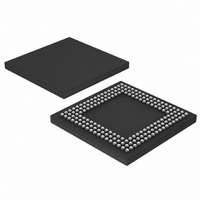
LPC2888FET180/D1,5 NXP Semiconductors, LPC2888FET180/D1,5 Datasheet - Page 24

LPC2888FET180/D1,5
Manufacturer Part Number
LPC2888FET180/D1,5
Description
IC ARM7 MCU 16K 180-TFBGA
Manufacturer
NXP Semiconductors
Series
LPC2800r
Datasheet
1.LPC2888FET180015.pdf
(43 pages)
Specifications of LPC2888FET180/D1,5
Core Processor
ARM7
Core Size
16/32-Bit
Speed
60MHz
Connectivity
EBI/EMI, I²C, IrDA, MMC, UART/USART, USB
Peripherals
DMA, I²S, LCD, WDT
Number Of I /o
85
Program Memory Size
1MB (1M x 8)
Program Memory Type
FLASH
Ram Size
64K x 8
Voltage - Supply (vcc/vdd)
1.7 V ~ 3.6 V
Data Converters
A/D 5x10b
Oscillator Type
External
Operating Temperature
-40°C ~ 85°C
Package / Case
180-TFBGA
Processor Series
LPC28
Core
ARM7TDMI-S
Data Bus Width
32 bit
Data Ram Size
64 KB
Interface Type
I2C, I2S, UART, USB
Maximum Clock Frequency
60 MHz
Number Of Programmable I/os
81
Number Of Timers
2
Operating Supply Voltage
1.8 V, 3.3 V
Maximum Operating Temperature
+ 85 C
Mounting Style
SMD/SMT
3rd Party Development Tools
MDK-ARM, RL-ARM, ULINK2
Development Tools By Supplier
OM10092
Minimum Operating Temperature
- 40 C
On-chip Adc
10 bit, 5 Channel
For Use With
OM10092 - EVAL BOARD FOR LPC288X
Lead Free Status / RoHS Status
Lead free / RoHS Compliant
Eeprom Size
-
Lead Free Status / Rohs Status
Details
Other names
935285219551
LPC2888FET180/D1-S
LPC2888FET180/D1-S
LPC2888FET180/D1-S
LPC2888FET180/D1-S
NXP Semiconductors
LPC2880_LPC2888_3
Preliminary data sheet
6.21.3 Crystal oscillator
6.21.4 PLLs
6.21.5 Power control and modes
The on-chip watchdog timer can cause a chip reset if not updated within a programmable
time interval. A status register allows software to determine if a reset was caused by the
watchdog timer. The watchdog timer can also be configured to generate an interrupt if
desired.
Software reset of many individual functional blocks may be performed via registers within
the CGU.
The main oscillator is the basis for the clocks most chip functions use by default. The
oscillator may be used with crystal frequencies from 1 MHz to 20 MHz.
The LPC2880/2888 includes two PLLs: the main PLL provides clocks to most chip
functions, and a high-speed PLL that can be used to generate faster clocks for selected
chip functions. Each PLL can be driven from several clock sources. These include the
main oscillator (1 MHz to 20 MHz), the RTC oscillator (32 kHz), the bit clock or word
select inputs of the I
the output clock from the other PLL.
The low power PLL takes the input clock and multiplies it up to a higher frequency (by 1 to
32), then divides it down (by 1, 2, 4, or 8) to provide the output clock used by the CGU.
The output frequency of this PLL can range from 10 MHz to 320 MHz. Functional blocks
may have limitations below this upper limit.
The high-speed PLL takes the input clock, optionally divides it down (by 1 to 256), then
multiplies it up to a higher frequency (by 1 to 1024), then divides it down (by 1 to 16) to
provide the output clock used by the CGU. The output frequency of this PLL can range
from 4.3 MHz to 550 MHz. Functional blocks may have limitations below this upper limit.
Power control on the LPC2880/2888 is accomplished by detailed control over the clocking
of each functional block via the CGU. The LPC2880/2888 includes a very versatile
clocking scheme that provides a great deal of control over performance and power usage.
On-chip functions are divided into 11 groups. Each group has a selection for one of
several basic clock sources. Graceful (glitch-free) switching between these clock sources
is provided.
Three of these functional groups include one fractional divider that allows any rate below
the selected clock to be derived. Three other functional groups include more than one
fractional divider, allowing several different slower clocks to be generated within the group.
Each function within the group can then be assigned to use any one of the generated
clocks.
Each function within any group can also be individually turned off by disabling the clock to
that function. When added to the versatile clock rate selection, this allows very detailed
control of power utilization.
Each function also can be configured to have clocks automatically turned on and off
based on a signal from the Event Router.
2
S input channel, the clock input from the SD/MMC card interface, or
16/32-bit ARM microcontrollers with external memory interface
Rev. 03 — 17 April 2008
LPC2880; LPC2888
© NXP B.V. 2008. All rights reserved.
24 of 43


