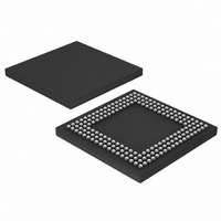
LPC2888FET180/D1,5 NXP Semiconductors, LPC2888FET180/D1,5 Datasheet - Page 16

LPC2888FET180/D1,5
Manufacturer Part Number
LPC2888FET180/D1,5
Description
IC ARM7 MCU 16K 180-TFBGA
Manufacturer
NXP Semiconductors
Series
LPC2800r
Datasheet
1.LPC2888FET180015.pdf
(43 pages)
Specifications of LPC2888FET180/D1,5
Core Processor
ARM7
Core Size
16/32-Bit
Speed
60MHz
Connectivity
EBI/EMI, I²C, IrDA, MMC, UART/USART, USB
Peripherals
DMA, I²S, LCD, WDT
Number Of I /o
85
Program Memory Size
1MB (1M x 8)
Program Memory Type
FLASH
Ram Size
64K x 8
Voltage - Supply (vcc/vdd)
1.7 V ~ 3.6 V
Data Converters
A/D 5x10b
Oscillator Type
External
Operating Temperature
-40°C ~ 85°C
Package / Case
180-TFBGA
Processor Series
LPC28
Core
ARM7TDMI-S
Data Bus Width
32 bit
Data Ram Size
64 KB
Interface Type
I2C, I2S, UART, USB
Maximum Clock Frequency
60 MHz
Number Of Programmable I/os
81
Number Of Timers
2
Operating Supply Voltage
1.8 V, 3.3 V
Maximum Operating Temperature
+ 85 C
Mounting Style
SMD/SMT
3rd Party Development Tools
MDK-ARM, RL-ARM, ULINK2
Development Tools By Supplier
OM10092
Minimum Operating Temperature
- 40 C
On-chip Adc
10 bit, 5 Channel
For Use With
OM10092 - EVAL BOARD FOR LPC288X
Lead Free Status / RoHS Status
Lead free / RoHS Compliant
Eeprom Size
-
Lead Free Status / Rohs Status
Details
Other names
935285219551
LPC2888FET180/D1-S
LPC2888FET180/D1-S
LPC2888FET180/D1-S
LPC2888FET180/D1-S
NXP Semiconductors
LPC2880_LPC2888_3
Preliminary data sheet
6.4.1 Features
6.6.1 Features
6.5 DC-to-DC converters
6.6 External memory controller
Programming the flash in a running application is accomplished via a register interface on
the APB bus. The flash module can generate an interrupt request when burning or erasing
is completed.
The flash memory contains a buffer to allow for faster execution. Information is read from
the flash 128 bits at a time. The buffer holds this entire amount, which can represent four
32-bit ARM instructions. These captured instructions can them be executed without flash
read delays, improving system performance.
The LPC2880/2888 include two DC-to-DC converters providing an on-chip power system
which allows the device to be powered by a standard single cell battery (AA or AAA for
example) as well as receive power from a USB port or other power source.
The LPC2880/2888 need two supply voltages, 3.3 V and 1.8 V, for various internal
functions. When power is available from a higher voltage source such as USB, two
internal Low Dropout regulators (LDO regulators) reduce the incoming voltage to the level
needed by the LPC2880/2888. When only a low voltage battery supply is available, two
DC-to-DC converters boost the voltage up to the needed levels. Switching between the
two modes is supported.
The LPC2880/2888 External Memory Controller (EMC) is a multi-port memory controller
that supports asynchronous static memory devices such as RAM, ROM and flash, as well
as dynamic memories such as Single Data Rate SDRAM. It complies with ARM’s AMBA.
•
•
•
•
•
•
•
•
•
•
Flash access for processor execution and data read is via the AHB bus.
Flash programming in a running application is via an APB register interface.
Initial programming or reprogramming is can be accomplished from the USB port.
Dynamic memory interface support including single data rate SDRAM.
Asynchronous static memory device support including RAM, ROM, and flash, with or
without asynchronous page mode.
Low transaction latency.
Read and write buffers to reduce latency and to improve performance.
8-bit and 16-bit static memory support.
16-bit SDRAM memory support.
Static memory features include:
– Asynchronous page mode read.
– Programmable wait states.
– Bus turnaround delay.
– Output enable and write enable delays.
– Extended wait.
16/32-bit ARM microcontrollers with external memory interface
Rev. 03 — 17 April 2008
LPC2880; LPC2888
© NXP B.V. 2008. All rights reserved.
16 of 43


