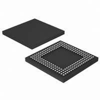
LPC2888FET180/D1,5 NXP Semiconductors, LPC2888FET180/D1,5 Datasheet - Page 18

LPC2888FET180/D1,5
Manufacturer Part Number
LPC2888FET180/D1,5
Description
IC ARM7 MCU 16K 180-TFBGA
Manufacturer
NXP Semiconductors
Series
LPC2800r
Datasheet
1.LPC2888FET180015.pdf
(43 pages)
Specifications of LPC2888FET180/D1,5
Core Processor
ARM7
Core Size
16/32-Bit
Speed
60MHz
Connectivity
EBI/EMI, I²C, IrDA, MMC, UART/USART, USB
Peripherals
DMA, I²S, LCD, WDT
Number Of I /o
85
Program Memory Size
1MB (1M x 8)
Program Memory Type
FLASH
Ram Size
64K x 8
Voltage - Supply (vcc/vdd)
1.7 V ~ 3.6 V
Data Converters
A/D 5x10b
Oscillator Type
External
Operating Temperature
-40°C ~ 85°C
Package / Case
180-TFBGA
Processor Series
LPC28
Core
ARM7TDMI-S
Data Bus Width
32 bit
Data Ram Size
64 KB
Interface Type
I2C, I2S, UART, USB
Maximum Clock Frequency
60 MHz
Number Of Programmable I/os
81
Number Of Timers
2
Operating Supply Voltage
1.8 V, 3.3 V
Maximum Operating Temperature
+ 85 C
Mounting Style
SMD/SMT
3rd Party Development Tools
MDK-ARM, RL-ARM, ULINK2
Development Tools By Supplier
OM10092
Minimum Operating Temperature
- 40 C
On-chip Adc
10 bit, 5 Channel
For Use With
OM10092 - EVAL BOARD FOR LPC288X
Lead Free Status / RoHS Status
Lead free / RoHS Compliant
Eeprom Size
-
Lead Free Status / Rohs Status
Details
Other names
935285219551
LPC2888FET180/D1-S
LPC2888FET180/D1-S
LPC2888FET180/D1-S
LPC2888FET180/D1-S
NXP Semiconductors
LPC2880_LPC2888_3
Preliminary data sheet
6.10.1 Features
6.10 General purpose timers
6.11 Watchdog timer
6.9 Event router
88 external and 11 internal LPC2880/2888 signals are connected to the Event Router
block. GPIO input pins, functional input pins, and even functional outputs can be
monitored by the Event Router.
Each signal can act as an interrupt source or a clock-enable for LPC2880/2888 modules,
with individual options for high- or low-level sensitivity or rising- or falling-edge sensitivity.
The outputs of the polarity and sensitivity logic can be read from Raw Status Registers 0
to 3.
Each active state is next masked/enabled by a “global” mask bit for that signal. The results
can be read from Pending Registers 0 to 3.
All 99 Pending signals are presented to each of the five output logic blocks. Each output
logic block includes a set of four Interrupt Output Mask Registers, each set totalling
99 bits, that control whether each signal applies to that output. These are logically ANDed
with the corresponding Pending signals, and the 99 results in each logic block are logically
ORed to make the output of the block. The 496 results can be read in the Interrupt Output
Pending Registers.
Outputs 0 to 3 are routed to the Interrupt Controller, in which each can be individually
enabled to cause an interrupt. Output 4 is routed to the Clock Generation Unit, in which it
can serve to enable clocking for selected clock domains. The five outputs can be read in
the Output Register.
The LPC2880/2888 contains two fully independent general purpose timers. Each timer is
a 32 bit wide down counter with a selectable prescaler. The prescaler allows either the
system clock to be used directly, or the clock to be divided by 16 or 256.
Two modes of operation are available, free-running and periodic timer. In periodic timer
mode, the counter will generate an interrupt at a constant interval. In free-running mode
the timer will overflow after reaching its zero value and continue to count down from the
maximum value.
The purpose of the watchdog timer is to interrupt and/or reset the microcontroller within a
reasonable amount of time if it enters an erroneous state. When enabled, the watchdog
will generate an interrupt or a system reset if the user program fails to reset the watchdog
within a predetermined amount of time. Alternatively, it can be used as an additional
general purpose Timer.
•
•
•
Two independent 32-bit timers.
Free-running or periodic operating modes.
Generate timed interrupts.
16/32-bit ARM microcontrollers with external memory interface
Rev. 03 — 17 April 2008
LPC2880; LPC2888
© NXP B.V. 2008. All rights reserved.
18 of 43


