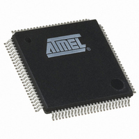
AT91SAM7X256B-AU Atmel, AT91SAM7X256B-AU Datasheet - Page 448

AT91SAM7X256B-AU
Manufacturer Part Number
AT91SAM7X256B-AU
Description
IC MCU 256KB FLASH 100LQFP
Manufacturer
Atmel
Series
AT91SAMr
Specifications of AT91SAM7X256B-AU
Core Processor
ARM7
Core Size
16/32-Bit
Speed
55MHz
Connectivity
CAN, Ethernet, I²C, SPI, SSC, UART/USART, USB
Peripherals
Brown-out Detect/Reset, DMA, POR, PWM, WDT
Number Of I /o
62
Program Memory Size
256KB (256K x 8)
Program Memory Type
FLASH
Ram Size
64K x 8
Voltage - Supply (vcc/vdd)
1.65 V ~ 1.95 V
Data Converters
A/D 8x10b
Oscillator Type
Internal
Operating Temperature
-40°C ~ 85°C
Package / Case
100-LQFP
Package
100LQFP
Device Core
ARM7TDMI
Family Name
91S
Maximum Speed
55 MHz
Operating Supply Voltage
1.8|3.3 V
Data Bus Width
32 Bit
Number Of Programmable I/os
62
Interface Type
CAN/Ethernet/SPI/I2S/TWI/USART/USB
On-chip Adc
8-chx10-bit
Number Of Timers
3
Controller Family/series
AT91SAM7xxxxx
No. Of I/o's
62
Ram Memory Size
64KB
Cpu Speed
55MHz
No. Of Timers
1
Rohs Compliant
Yes
Cpu Family
91S
Device Core Size
32b
Frequency (max)
55MHz
Total Internal Ram Size
64KB
# I/os (max)
62
Number Of Timers - General Purpose
3
Operating Supply Voltage (typ)
1.8/3.3V
Operating Supply Voltage (max)
1.95/3.6V
Operating Supply Voltage (min)
1.65/3V
Instruction Set Architecture
RISC
Operating Temp Range
-40C to 85C
Operating Temperature Classification
Industrial
Mounting
Surface Mount
Pin Count
100
Package Type
LQFP
Lead Free Status / RoHS Status
Lead free / RoHS Compliant
Eeprom Size
-
Lead Free Status / Rohs Status
Compliant
Available stocks
Company
Part Number
Manufacturer
Quantity
Price
Company:
Part Number:
AT91SAM7X256B-AU
Manufacturer:
Atmel
Quantity:
1 800
Part Number:
AT91SAM7X256B-AU
Manufacturer:
ATMEL/爱特梅尔
Quantity:
20 000
- Current page: 448 of 687
- Download datasheet (11Mb)
34.2
Figure 34-1. Block Diagram
448
MCK
UDPCK
udp_int
external_resume
Block Diagram
AT91SAM7X512/256/128 Preliminary
Atmel Bridge
MCU
APB
Bus
to
Access to the UDP is via the APB bus interface. Read and write to the data FIFO are done by
reading and writing 8-bit values to APB registers.
The UDP peripheral requires two clocks: one peripheral clock used by the MCK domain and a
48 MHz clock used by the 12 MHz domain.
A USB 2.0 full-speed pad is embedded and controlled by the Serial Interface Engine (SIE).
The signal external_resume is optional. It allows the UDP peripheral to wake up once in system
mode. The host is then notified that the device asks for a resume. This optional feature must be
also negotiated with the host during the enumeration.
U
e
n
e
a
e
s
c
r
I
t
r
f
W
a
p
p
e
Master Clock
Domain
r
r
USB Device
RAM
FIFO
Dual
Port
Recovered 12 MHz
Domain
W
a
p
p
e
r
r
Suspend/Resume Logic
12 MHz
Interface
Engine
Serial
SIE
txoen
eopn
txd
rxdm
rxd
rxdp
6120H–ATARM–17-Feb-09
Transceiver
Embedded
USB
DM
DP
Related parts for AT91SAM7X256B-AU
Image
Part Number
Description
Manufacturer
Datasheet
Request
R

Part Number:
Description:
KIT EVAL FOR AT91SAM7X256/128
Manufacturer:
Atmel
Datasheet:

Part Number:
Description:
MCU, MPU & DSP Development Tools KICKSTART KIT ATMEL AT91SAM7X
Manufacturer:
IAR Systems

Part Number:
Description:
MCU ARM9 64K SRAM 144-LFBGA
Manufacturer:
Atmel
Datasheet:

Part Number:
Description:
IC ARM7 MCU FLASH 256K 100LQFP
Manufacturer:
Atmel
Datasheet:

Part Number:
Description:
IC ARM9 MPU 217-LFBGA
Manufacturer:
Atmel
Datasheet:

Part Number:
Description:
MCU ARM9 ULTRA LOW PWR 217-LFBGA
Manufacturer:
Atmel
Datasheet:

Part Number:
Description:
MCU ARM9 324-TFBGA
Manufacturer:
Atmel
Datasheet:

Part Number:
Description:
IC MCU ARM9 SAMPLING 217CBGA
Manufacturer:
Atmel
Datasheet:

Part Number:
Description:
IC ARM9 MCU 217-LFBGA
Manufacturer:
Atmel
Datasheet:

Part Number:
Description:
IC ARM9 MCU 208-PQFP
Manufacturer:
Atmel
Datasheet:

Part Number:
Description:
MCU ARM 512K HS FLASH 100-LQFP
Manufacturer:
Atmel
Datasheet:

Part Number:
Description:
MCU ARM 512K HS FLASH 100-TFBGA
Manufacturer:
Atmel
Datasheet:

Part Number:
Description:
IC ARM9 MCU 200 MHZ 324-TFBGA
Manufacturer:
Atmel
Datasheet:

Part Number:
Description:
IC ARM MCU 16BIT 128K 256BGA
Manufacturer:
Atmel
Datasheet:

Part Number:
Description:
IC ARM7 MCU 32BIT 128K 64LQFP
Manufacturer:
Atmel
Datasheet:


