AT91SAM7X256B-AU Atmel, AT91SAM7X256B-AU Datasheet
AT91SAM7X256B-AU
Specifications of AT91SAM7X256B-AU
Available stocks


Related parts for AT91SAM7X256B-AU


AT91SAM7X256B-AU Summary of contents
Page 1
... Provides Reset or Interrupt Signals to the System – Counter May Be Stopped While the Processor is in Debug State or in Idle Mode ® ® Thumb Processor Product Description AT91SAM7X512 AT91SAM7X256 AT91SAM7X128 Preliminary Summary NOTE: This is a summary document. The complete document is available on the Atmel website at www.atmel.com. 6120FS–ATARM–17-Feb-09 ...
Page 2
... Double PWM Generation, Capture/Waveform Mode, Up/Down Capability • One Four-channel 16-bit Power Width Modulation Controller (PWMC) • One Two-wire Interface (TWI) – Master Mode Support Only, All Two-wire Atmel EEPROMs and I • One 8-channel 10-bit Analog-to-Digital Converter, Four Channels Multiplexed with Digital I/Os ® • ...
Page 3
... AT91SAM7X512/256/128 Preliminary Summary 1. Description Atmel's AT91SAM7X512/256/128 is a member of a series of highly integrated Flash microcon- trollers based on the 32-bit ARM RISC processor. It features 512/256/128 Kbyte high-speed Flash and 128/64/32 Kbyte SRAM, a large set of peripherals, including an 802.3 Ethernet MAC and a CAN controller. A complete set of system functions minimizes the number of external components ...
Page 4
AT91SAM7X512/256/128 Block Diagram Figure 2-1. TDO TMS TCK JTAGSEL TST FIQ IRQ0-IRQ1 DRXD DTXD PCK0-PCK3 PLLRC XIN XOUT VDDCORE VDDFLASH VDDCORE NRST RXD0 TXD0 SCK0 RTS0 CTS0 RXD1 TXD1 SCK1 RTS1 CTS1 DCD1 DSR1 DTR1 SPI0_NPCS0 SPI0_NPCS1 SPI0_NPCS2 SPI0_NPCS3 ...
Page 5
AT91SAM7X512/256/128 Preliminary Summary 3. Signal Description Table 3-1. Signal Description List Signal Name Function Voltage Regulator and ADC Power VDDIN Supply Input VDDOUT Voltage Regulator Output VDDFLASH Flash and USB Power Supply VDDIO I/O Lines Power Supply VDDCORE Core Power ...
Page 6
Table 3-1. Signal Description List (Continued) Signal Name Function DDM USB Device Port Data - DDP USB Device Port Data + SCK0 - SCK1 Serial Clock TXD0 - TXD1 Transmit Data RXD0 - RXD1 Receive Data RTS0 - RTS1 Request ...
Page 7
AT91SAM7X512/256/128 Preliminary Summary Table 3-1. Signal Description List (Continued) Signal Name Function AD0-AD3 Analog Inputs AD4-AD7 Analog Inputs ADTRG ADC Trigger ADVREF ADC Reference PGMEN0-PGMEN1 Programming Enabling PGMM0-PGMM3 Programming Mode PGMD0-PGMD15 Programming Data PGMRDY Programming Ready PGMNVALID Data Direction PGMNOE ...
Page 8
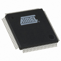
Package The AT91SAM7X512/256/128 is available in 100-lead LQFP Green and 100-ball TFBGA RoHS- compliant packages. 4.1 100-lead LQFP Package Outline Figure 4-1 tion is given in the Mechanical Characteristics section. Figure 4-1. AT91SAM7X512/256/128 Preliminary 8 shows the orientation of ...
Page 9
AT91SAM7X512/256/128 Preliminary Summary 4.2 100-lead LQFP Pinout Table 4-1. Pinout in 100-lead LQFP Package 1 ADVREF 26 2 GND 27 3 AD4 28 4 AD5 29 5 AD6 30 6 AD7 31 7 VDDOUT 32 8 VDDIN 33 9 PB27/AD0 ...
Page 10
TFBGA Package Outline Figure 4-2 description is given in the Mechanical Characteristics section of the full datasheet. Figure 4-2. 4.4 100-ball TFBGA Pinout Pinout in 100-ball TFBGA Package Pin Signal Name Pin A1 PA22/PGMD10 C6 A2 PA21/PGMD9 C7 ...
Page 11
AT91SAM7X512/256/128 Preliminary Summary 5. Power Considerations 5.1 Power Supplies The AT91SAM7X512/256/128 has six types of power supply pins and integrates a voltage regu- lator, allowing the device to be supplied with only one voltage. The six power supply pin types ...
Page 12
Adequate input supply decoupling is mandatory for VDDIN in order to improve startup stability and reduce source voltage drop. The input decoupling capacitor should be placed close to the chip. For example, two capacitors can be used in parallel: 100 ...
Page 13
AT91SAM7X512/256/128 Preliminary Summary 6. I/O Lines Considerations 6.1 JTAG Port Pins TMS, TDI and TCK are schmitt trigger inputs and are not 5-V tolerant. TMS, TDI and TCK do not integrate a pull-up resistor. TDO is an output, driven at ...
Page 14
PIO Controller Lines All the I/O lines, PA0 to PA30 and PB0 to PB30, are 5V-tolerant and all integrate a programma- ble pull-up resistor. Programming of this pull-up resistor is performed independently for each I/O line through the PIO ...
Page 15
AT91SAM7X512/256/128 Preliminary Summary 7. Processor and Architecture 7.1 ARM7TDMI Processor • RISC processor based on ARMv4T Von Neumann architecture – Runs MHz, providing 0.9 MIPS/MHz • Two instruction sets – ARM high-performance 32-bit instruction set – ...
Page 16
Embedded Flash Controller – Embedded Flash interface three programmable wait states – Prefetch buffer, buffering and anticipating the 16-bit requests, reducing the required wait states – Key-protected program, erase and lock/unlock sequencer – Single command for erasing, ...
Page 17
AT91SAM7X512/256/128 Preliminary Summary 8. Memories 8.1 AT91SAM7X512 • 512 Kbytes of dual-plane Flash Memory – 2 contiguous banks of 1024 pages of 256 bytes – Fast access time, 30 MHz single-cycle access in Worst Case conditions – Page programming time: ...
Page 18
Figure 8-1. AT91SAM7X512/256/128 Memory Mapping Address Memory Space 0x0000 0000 Internal Memories 256 MBytes 0x0FFF FFFF 0x1000 0000 Undefined 14 x 256 MBytes (Abort) 3,584 MBytes 0xEFFF FFFF 0xF000 0000 Internal Peripherals 256 MBytes 0xFFFF FFFF AT91SAM7X512/256/128 Preliminary 18 Internal ...
Page 19
AT91SAM7X512/256/128 Preliminary Summary 8.4 Memory Mapping 8.4.1 Internal SRAM • The AT91SAM7X512 embeds a high-speed 128 Kbyte SRAM bank. • The AT91SAM7X256 embeds a high-speed 64 Kbyte SRAM bank. • The AT91SAM7X128 embeds a high-speed 32 Kbyte SRAM bank. After ...
Page 20
Figure 8-3. 8.5 Embedded Flash 8.5.1 Flash Overview • The Flash of the AT91SAM7X512 is organized in two banks (dual plane) of 1024 pages of 256 bytes. The 524,288 bytes are organized in 32-bit words. • The Flash of the ...
Page 21
AT91SAM7X512/256/128 Preliminary Summary plane may be performed even while program or erase functions are being executed in the other memory plane. One EFC is embedded in the AT91SAM7X256/128 to control the single plane of 256/128 KBytes. 8.5.3 Lock Regions 8.5.3.1 ...
Page 22
Flash Programming Interface, is forbidden. This ensures the confidentiality of the code pro- grammed in the Flash. This security bit can only be enabled, through the Command “Set Security Bit” of the EFC User Interface. Disabling the security bit can ...
Page 23
AT91SAM7X512/256/128 Preliminary Summary • Communication via the USB Device Port is limited to an 18.432 MHz crystal. The SAM-BA Boot provides an interface with SAM-BA Graphic User Interface (GUI). The SAM-BA Boot is in ROM and is mapped at address ...
Page 24
System Controller The System Controller manages all vital blocks of the microcontroller: interrupts, clocks, power, time, debug and reset. The System Controller peripherals are all mapped to the highest 4 Kbytes of address space, between addresses 0xFFFF F000 and ...
Page 25
AT91SAM7X512/256/128 Preliminary Summary Figure 9-1. NRST XOUT PLLRC PA0-PA30 PB0-PB30 6120FS–ATARM–17-Feb-09 System Controller Block Diagram System Controller irq0-irq1 Advanced fiq Interrupt Controller periph_irq[2..19] pit_irq rtt_irq wdt_irq dbgu_irq pmc_irq rstc_irq efc_irq MCK Debug periph_nreset Unit dbgu_rxd Periodic MCK debug Interval periph_nreset ...
Page 26
Reset Controller • Based on one power-on reset cell and one brownout detector • Status of the last reset, either Power-up Reset, Software Reset, User Reset, Watchdog Reset, Brownout Reset • Controls the internal resets and the NRST pin ...
Page 27
AT91SAM7X512/256/128 Preliminary Summary 9.2 Clock Generator The Clock Generator embeds one low-power RC Oscillator, one Main Oscillator and one PLL with the following characteristics: • RC Oscillator ranges between 22 KHz and 42 KHz • Main Oscillator frequency ranges between ...
Page 28
Power Management Controller The Power Management Controller uses the Clock Generator outputs to provide: • the Processor Clock PCK • the Master Clock MCK • the USB Clock UDPCK • all the peripheral clocks, independently controllable • four programmable ...
Page 29
AT91SAM7X512/256/128 Preliminary Summary – Higher priority interrupts can be served during service of lower priority interrupt • Vectoring – Optimizes interrupt service routine branch and execution – One 32-bit vector register per interrupt source – Interrupt vector register reads the ...
Page 30
Real-time Timer • 32-bit free-running counter with alarm running on prescaled SLCK • Programmable 16-bit prescaler for SLCK accuracy compensation 9.9 PIO Controllers • Two PIO Controllers, each controlling 31 I/O lines • Fully programmable through set/clear registers • ...
Page 31
AT91SAM7X512/256/128 Preliminary Summary 10. Peripherals 10.1 User Interface The User Peripherals are mapped in the 256 Mbytes of address space between 0xF000 0000 and 0xFFFF EFFF. Each peripheral is allocated 16 Kbytes of address space. A complete memory map is ...
Page 32
Peripheral Multiplexing on PIO Lines The AT91SAM7X512/256/128 features two PIO controllers, PIOA and PIOB, that multiplex the I/O lines of the peripheral set. Each PIO Controller controls 31 lines. Each line can be assigned to one of two peripheral ...
Page 33
AT91SAM7X512/256/128 Preliminary Summary 10.4 PIO Controller A Multiplexing Table 10-2. Multiplexing on PIO Controller A PIO Controller A I/O Line Peripheral A PA0 RXD0 PA1 TXD0 PA2 SCK0 PA3 RTS0 PA4 CTS0 PA5 RXD1 PA6 TXD1 PA7 SCK1 PA8 RTS1 ...
Page 34
PIO Controller B Multiplexing Table 10-3. Multiplexing on PIO Controller B PIO Controller B I/O Line Peripheral A PB0 ETXCK/EREFCK PB1 ETXEN PB2 ETX0 PB3 ETX1 PB4 ECRS PB5 ERX0 PB6 ERX1 PB7 ERXER PB8 EMDC PB9 EMDIO PB10 ...
Page 35
AT91SAM7X512/256/128 Preliminary Summary 10.6 Ethernet MAC • DMA Master on Receive and Transmit Channels • Compatible with IEEE Standard 802.3 • 10 and 100 Mbit/s operation • Full- and half-duplex operation • Statistics Counter Registers • MII/RMII interface to the ...
Page 36
One, two or three bytes internal address registers for easy Serial Memory access • 7-bit or 10-bit slave addressing • Sequential read/write operations 10.9 USART • Programmable Baud Rate Generator • 9-bit full-duplex synchronous or asynchronous serial ...
Page 37
AT91SAM7X512/256/128 Preliminary Summary – Pulse generation – Delay timing – Pulse Width Modulation – Up/down capabilities • Each channel is user-configurable and contains: – Three external clock inputs • Five internal clock inputs, as defined in Table 10-4. TC Clock ...
Page 38
CAN Controller • Fully compliant with CAN 2.0A and 2.0B • Bit rates up to 1Mbit/s • Eight object oriented mailboxes each with the following properties: – CAN Specification 2.0 Part A or 2.0 Part B Programmable for each ...
Page 39
AT91SAM7X512/256/128 Preliminary Summary 11. Package Drawings Figure 11-1. LQFP Package Drawing 6120FS–ATARM–17-Feb-09 39 ...
Page 40
Table 11-1. Symbol θ1 θ2 θ aaa bbb ccc ddd AT91SAM7X512/256/128 Preliminary 40 100-lead LQFP Package Dimensions Millimeter Min Nom Max 1.60 ...
Page 41
AT91SAM7X512/256/128 Preliminary Summary Figure 11-2. TFBGA Package Drawing All dimensions are in mm 6120FS–ATARM–17-Feb-09 41 ...
Page 42
... Ordering Information Table 12-1. Ordering Information MLR A Ordering Code MLR B Ordering Code AT91SAM7X512-AU AT91SAM7X512-CU AT91SAM7X256-AU AT91SAM7X256B-AU AT91SAM7X256-CU AT91SAM7X256B-CU AT91SAM7X128-AU AT91SAM7X128B-AU AT91SAM7X128-CU AT91SAM7X128B-CU AT91SAM7X512/256/128 Preliminary 42 Package LQFP 100 – TFBGA 100 LQFP 100 TFBGA 100 LQFP 100 TFBGA 100 Temperature Package Type ...
Page 43
AT91SAM7X512/256/128 Preliminary Summary Revision History Table 12-2. Revision History Doc. Rev Comments 6120AS First issue - Unqualified on Intranet Legal page updated.Qualified on Intranet 6120BS Corrections to maintain consistency with full datasheet: In “Features” on page PDC channels, removed Wake-on-LAN ...
Page 44
... Revision History Doc. Rev Comments 6120ES “Features” ,TWI updated to include Atmel TWI compatibility with I2C Standard. Section 10.8 ”Two-wire Interface”, updated. Section 7.4 ”Peripheral DMA Section 10.11 ”Timer Counter”, The TC has Two output compare or one input capture per channel. ...
Page 45
... Disclaimer: The information in this document is provided in connection with Atmel products. No license, express or implied, by estoppel or otherwise, to any intellectual property right is granted by this document or in connection with the sale of Atmel products. EXCEPT AS SET FORTH IN ATMEL’S TERMS AND CONDI- TIONS OF SALE LOCATED ON ATMEL’S WEB SITE, ATMEL ASSUMES NO LIABILITY WHATSOEVER AND DISCLAIMS ANY EXPRESS, IMPLIED OR STATUTORY WARRANTY RELATING TO ITS PRODUCTS INCLUDING, BUT NOT LIMITED TO, THE IMPLIED WARRANTY OF MERCHANTABILITY, FITNESS FOR A PARTICULAR PURPOSE, OR NON-INFRINGEMENT ...