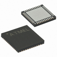
ATMEGA644P-A15MZ Atmel, ATMEGA644P-A15MZ Datasheet - Page 87

ATMEGA644P-A15MZ
Manufacturer Part Number
ATMEGA644P-A15MZ
Description
MCU AVR 64KB FLASH 16MHZ 44QFN
Manufacturer
Atmel
Series
AVR® ATmegar
Specifications of ATMEGA644P-A15MZ
Package / Case
44-VQFN Exposed Pad
Voltage - Supply (vcc/vdd)
2.7 V ~ 5.5 V
Operating Temperature
-40°C ~ 125°C
Speed
16MHz
Number Of I /o
32
Eeprom Size
2K x 8
Core Processor
AVR
Program Memory Type
FLASH
Ram Size
4K x 8
Program Memory Size
64KB (64K x 8)
Data Converters
A/D 8x10b
Oscillator Type
Internal
Peripherals
Brown-out Detect/Reset, POR, PWM, WDT
Connectivity
I²C, SPI, UART/USART
Core Size
8-Bit
Lead Free Status / RoHS Status
Lead free / RoHS Compliant
Available stocks
Company
Part Number
Manufacturer
Quantity
Price
Company:
Part Number:
ATMEGA644P-A15MZ
Manufacturer:
ATMEL
Quantity:
3 500
Part Number:
ATMEGA644P-A15MZ
Manufacturer:
ATMEL/爱特梅尔
Quantity:
20 000
- Current page: 87 of 377
- Download datasheet (7Mb)
ATmega164P/324P/644P
The alternate pin configuration is as follows:
• OC2A/PCINT31 – Port D, Bit 7
OC2A, Output Compare Match A output: The PD7 pin can serve as an external output for the
Timer/Counter2 Output Compare A. The pin has to be configured as an output (DDD7 set (one))
to serve this function. The OC2A pin is also the output pin for the PWM mode timer function.
PCINT31, Pin Change Interrupt Source 31:The PD7 pin can serve as an external interrupt
source.
• ICP1/OC2B/PCINT30 – Port D, Bit 6
ICP1, Input Capture Pin 1: The PD6 pin can act as an input capture pin for Timer/Counter1.
OC2B, Output Compare Match B output: The PD6 pin can serve as an external output for the
Timer/Counter2 Output Compare B. The pin has to be configured as an output (DDD6 set (one))
to serve this function. The OC2B pin is also the output pin for the PWM mode timer function.
PCINT30, Pin Change Interrupt Source 30: The PD6 pin can serve as an external interrupt
source.
• OC1A/PCINT29 – Port D, Bit 5
OC1A, Output Compare Match A output: The PD5 pin can serve as an external output for the
Timer/Counter1 Output Compare A. The pin has to be configured as an output (DDD5 set (one))
to serve this function. The OC1A pin is also the output pin for the PWM mode timer function.
PCINT29, Pin Change Interrupt Source 29: The PD5 pin can serve as an external interrupt
source.
• OC1B/XCK1/PCINT28 – Port D, Bit 4
OC1B, Output Compare Match B output: The PB4 pin can serve as an external output for the
Timer/Counter1 Output Compare B. The pin has to be configured as an output (DDD4 set (one))
to serve this function. The OC1B pin is also the output pin for the PWM mode timer function.
XCK1, USART1 External clock. The Data Direction Register (DDB4) controls whether the clock
is output (DDD4 set “one”) or input (DDD4 cleared). The XCK4 pin is active only when the
USART1 operates in Synchronous mode.
PCINT28, Pin Change Interrupt Source 28: The PD4 pin can serve as an external interrupt
source.
• INT1/TXD1/PCINT27 – Port D, Bit 3
INT1, External Interrupt source 1. The PD3 pin can serve as an external interrupt source to the
MCU.
TXD1, Transmit Data (Data output pin for the USART1). When the USART1 Transmitter is
enabled, this pin is configured as an output regardless of the value of DDD3.
PCINT27, Pin Change Interrupt Source 27: The PD3 pin can serve as an external interrupt
source.
87
7674F–AVR–09/09
Related parts for ATMEGA644P-A15MZ
Image
Part Number
Description
Manufacturer
Datasheet
Request
R

Part Number:
Description:
Manufacturer:
Atmel Corporation
Datasheet:

Part Number:
Description:
Manufacturer:
Atmel Corporation
Datasheet:

Part Number:
Description:
IC MCU AVR 64K FLASH 44-TQFP
Manufacturer:
Atmel
Datasheet:

Part Number:
Description:
IC MCU AVR 64K FLASH 44-QFN
Manufacturer:
Atmel
Datasheet:

Part Number:
Description:
MCU AVR 64K FLASH 20MHZ 44-TQFP
Manufacturer:
Atmel
Datasheet:

Part Number:
Description:
IC MCU AVR 64K FLASH 40-DIP
Manufacturer:
Atmel
Datasheet:

Part Number:
Description:
MCU AVR 64K FLASH 20MHZ 44TQFP
Manufacturer:
Atmel
Datasheet:

Part Number:
Description:
MCU AVR 64K FLASH 20MHZ 44QFN
Manufacturer:
Atmel
Datasheet:

Part Number:
Description:
MCU AVR 64K FLASH 20MHZ 44-QFN
Manufacturer:
Atmel
Datasheet:

Part Number:
Description:
MCU AVR 64K FLASH 20MHZ 40-PDIP
Manufacturer:
Atmel
Datasheet:

Part Number:
Description:
MCU AVR 64K FLASH 15MHZ 44-TQFP
Manufacturer:
Atmel
Datasheet:


