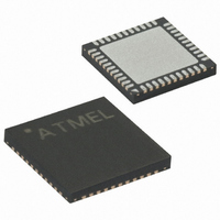
ATMEGA644P-A15MZ Atmel, ATMEGA644P-A15MZ Datasheet - Page 175

ATMEGA644P-A15MZ
Manufacturer Part Number
ATMEGA644P-A15MZ
Description
MCU AVR 64KB FLASH 16MHZ 44QFN
Manufacturer
Atmel
Series
AVR® ATmegar
Specifications of ATMEGA644P-A15MZ
Package / Case
44-VQFN Exposed Pad
Voltage - Supply (vcc/vdd)
2.7 V ~ 5.5 V
Operating Temperature
-40°C ~ 125°C
Speed
16MHz
Number Of I /o
32
Eeprom Size
2K x 8
Core Processor
AVR
Program Memory Type
FLASH
Ram Size
4K x 8
Program Memory Size
64KB (64K x 8)
Data Converters
A/D 8x10b
Oscillator Type
Internal
Peripherals
Brown-out Detect/Reset, POR, PWM, WDT
Connectivity
I²C, SPI, UART/USART
Core Size
8-Bit
Lead Free Status / RoHS Status
Lead free / RoHS Compliant
Available stocks
Company
Part Number
Manufacturer
Quantity
Price
Company:
Part Number:
ATMEGA644P-A15MZ
Manufacturer:
ATMEL
Quantity:
3 500
Part Number:
ATMEGA644P-A15MZ
Manufacturer:
ATMEL/爱特梅尔
Quantity:
20 000
- Current page: 175 of 377
- Download datasheet (7Mb)
17.4.3
17.4.4
7674F–AVR–09/09
External Clock
Synchronous Clock Operation
External clocking is used by the synchronous slave modes of operation. The description in this
section refers to
External clock input from the XCKn pin is sampled by a synchronization register to minimize the
chance of meta-stability. The output from the synchronization register must then pass through
an edge detector before it can be used by the Transmitter and Receiver. This process intro-
duces a two CPU clock period delay and therefore the maximum external XCKn clock frequency
is limited by the following equation:
Note that f
add some margin to avoid possible loss of data due to frequency variations.
When synchronous mode is used (UMSELn = 1), the XCKn pin will be used as either clock input
(Slave) or clock output (Master). The dependency between the clock edges and data sampling
or data change is the same. The basic principle is that data input (on RxDn) is sampled at the
opposite XCKn clock edge of the edge the data output (TxDn) is changed.
Figure 17-3. Synchronous Mode XCKn Timing.
The UCPOLn bit UCRSC selects which XCKn clock edge is used for data sampling and which is
used for data change. As
be changed at rising XCKn edge and sampled at falling XCKn edge. If UCPOLn is set, the data
will be changed at falling XCKn edge and sampled at rising XCKn edge.
UCPOL = 1
UCPOL = 0
osc
depends on the stability of the system clock source. It is therefore recommended to
Figure 17-2 on page 173
RxD / TxD
RxD / TxD
XCK
XCK
Figure 17-3 on page 175
for details.
f
XCK
f
---------- -
ATmega164P/324P/644P
OSC
4
shows, when UCPOLn is zero the data will
Sample
Sample
175
Related parts for ATMEGA644P-A15MZ
Image
Part Number
Description
Manufacturer
Datasheet
Request
R

Part Number:
Description:
Manufacturer:
Atmel Corporation
Datasheet:

Part Number:
Description:
Manufacturer:
Atmel Corporation
Datasheet:

Part Number:
Description:
IC MCU AVR 64K FLASH 44-TQFP
Manufacturer:
Atmel
Datasheet:

Part Number:
Description:
IC MCU AVR 64K FLASH 44-QFN
Manufacturer:
Atmel
Datasheet:

Part Number:
Description:
MCU AVR 64K FLASH 20MHZ 44-TQFP
Manufacturer:
Atmel
Datasheet:

Part Number:
Description:
IC MCU AVR 64K FLASH 40-DIP
Manufacturer:
Atmel
Datasheet:

Part Number:
Description:
MCU AVR 64K FLASH 20MHZ 44TQFP
Manufacturer:
Atmel
Datasheet:

Part Number:
Description:
MCU AVR 64K FLASH 20MHZ 44QFN
Manufacturer:
Atmel
Datasheet:

Part Number:
Description:
MCU AVR 64K FLASH 20MHZ 44-QFN
Manufacturer:
Atmel
Datasheet:

Part Number:
Description:
MCU AVR 64K FLASH 20MHZ 40-PDIP
Manufacturer:
Atmel
Datasheet:

Part Number:
Description:
MCU AVR 64K FLASH 15MHZ 44-TQFP
Manufacturer:
Atmel
Datasheet:


