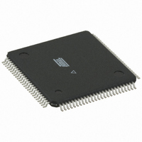
ATMEGA1280-16AUR Atmel, ATMEGA1280-16AUR Datasheet - Page 29

ATMEGA1280-16AUR
Manufacturer Part Number
ATMEGA1280-16AUR
Description
MCU AVR 128K FLASH 16MHZ 100TQFP
Manufacturer
Atmel
Series
AVR® ATmegar
Specifications of ATMEGA1280-16AUR
Core Processor
AVR
Core Size
8-Bit
Speed
16MHz
Connectivity
EBI/EMI, I²C, SPI, UART/USART
Peripherals
Brown-out Detect/Reset, POR, PWM, WDT
Number Of I /o
86
Program Memory Size
128KB (64K x 16)
Program Memory Type
FLASH
Eeprom Size
4K x 8
Ram Size
8K x 8
Voltage - Supply (vcc/vdd)
2.7 V ~ 5.5 V
Data Converters
A/D 16x10b
Oscillator Type
Internal
Operating Temperature
-40°C ~ 85°C
Package / Case
100-TQFP, 100-VQFP
For Use With
ATSTK600-TQFP100 - STK600 SOCKET/ADAPTER 100-TQFPATSTK503 - STARTER KIT AVR EXP MODULE 100P
Lead Free Status / RoHS Status
Lead free / RoHS Compliant
Available stocks
Company
Part Number
Manufacturer
Quantity
Price
- Current page: 29 of 444
- Download datasheet (10Mb)
8.1.1
8.1.2
2549M–AVR–09/10
Using the External Memory Interface
Address Latch Requirements
The interface consists of:
•
•
•
•
The control bits for the External Memory Interface are located in two registers, the External
Memory Control Register A – XMCRA, and the External Memory Control Register B – XMCRB.
When the XMEM interface is enabled, the XMEM interface will override the setting in the data
direction registers that corresponds to the ports dedicated to the XMEM interface. For details
about the port override, see the alternate functions in section
interface will auto-detect whether an access is internal or external. If the access is external, the
XMEM interface will output address, data, and the control signals on the ports according to
ure 8-3 on page 31
high-to-low, there is a valid address on AD7:0. ALE is low during a data transfer. When the
XMEM interface is enabled, also an internal access will cause activity on address, data and ALE
ports, but the RD and WR strobes will not toggle during internal access. When the External
Memory Interface is disabled, the normal pin and data direction settings are used. Note that
when the XMEM interface is disabled, the address space above the internal SRAM boundary is
not mapped into the internal SRAM.
SRAM to the AVR using an octal latch (typically “74 × 573” or equivalent) which is transparent
when G is high.
Due to the high-speed operation of the XRAM interface, the address latch must be selected with
care for system frequencies above 8 MHz @ 4V and 4 MHz @ 2.7V. When operating at condi-
tions above these frequencies, the typical old style 74HC series latch becomes inadequate. The
External Memory Interface is designed in compliance to the 74AHC series latch. However, most
latches can be used as long they comply with the main timing parameters. The main parameters
for the address latch are:
•
•
•
The External Memory Interface is designed to guaranty minimum address hold time after G is
asserted low of t
9 through Tables 30-16 on pages 378 - 381. The D-to-Q propagation delay (t
into consideration when calculating the access time requirement of the external component. The
data setup time before G low (t
wiring delay (dependent on the capacitive load).
AD7:0: Multiplexed low-order address bus and data bus.
ALE: Address latch enable.
RD: Read strobe.
WR: Write strobe.
D to Q propagation delay (t
Data setup time before G low (t
Data (address) hold time after G low (
• A15:8: High-order address bus (configurable number of bits).
h
= 5 ns. Refer to t
(this figure shows the wave forms without wait-states). When ALE goes from
SU
PD
ATmega640/1280/1281/2560/2561
) must not exceed address valid to ALE low (t
).
LAXX_LD
SU
Figure 8-2 on page 30
).
/t
TH
LLAXX_ST
).
in “External Data Memory Timing” Tables 30-
illustrates how to connect an external
“I/O-Ports” on page
PD
AVLLC
) must be taken
70. The XMEM
) minus PCB
Fig-
29
Related parts for ATMEGA1280-16AUR
Image
Part Number
Description
Manufacturer
Datasheet
Request
R

Part Number:
Description:
Manufacturer:
Atmel Corporation
Datasheet:

Part Number:
Description:
IC MCU AVR 128K FLASH 100-CBGA
Manufacturer:
Atmel
Datasheet:

Part Number:
Description:
IC MCU AVR 128K FLASH 100-TQFP
Manufacturer:
Atmel
Datasheet:

Part Number:
Description:
MCU AVR 128K FLASH 16MHZ 100CBGA
Manufacturer:
Atmel
Datasheet:

Part Number:
Description:
Manufacturer:
ATMEL Corporation
Datasheet:

Part Number:
Description:
Microcontroller with 128K bytes In-system programmable flash, 8 MHz, power supply =2.7 - 5.5V
Manufacturer:
ATMEL Corporation
Datasheet:

Part Number:
Description:
IC AVR MCU 128K 16MHZ 5V 64TQFP
Manufacturer:
Atmel
Datasheet:

Part Number:
Description:
IC AVR MCU 128K 16MHZ 5V 64-QFN
Manufacturer:
Atmel
Datasheet:

Part Number:
Description:
IC AVR MCU 128K 16MHZ COM 64-QFN
Manufacturer:
Atmel
Datasheet:

Part Number:
Description:
IC AVR MCU 128K 16MHZ 64-TQFP
Manufacturer:
Atmel
Datasheet:

Part Number:
Description:
IC AVR MCU 128K 16MHZ 64-TQFP
Manufacturer:
Atmel
Datasheet:


