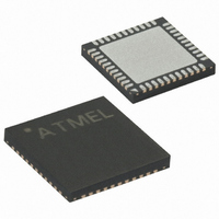
ATMEGA644V-10MU Atmel, ATMEGA644V-10MU Datasheet - Page 243

ATMEGA644V-10MU
Manufacturer Part Number
ATMEGA644V-10MU
Description
IC AVR MCU FLASH 64K 44-QFN
Manufacturer
Atmel
Series
AVR® ATmegar
Specifications of ATMEGA644V-10MU
Core Processor
AVR
Core Size
8-Bit
Speed
10MHz
Connectivity
I²C, SPI, UART/USART
Peripherals
Brown-out Detect/Reset, POR, PWM, WDT
Number Of I /o
32
Program Memory Size
64KB (32K x 16)
Program Memory Type
FLASH
Eeprom Size
2K x 8
Ram Size
4K x 8
Voltage - Supply (vcc/vdd)
1.8 V ~ 5.5 V
Data Converters
A/D 8x10b
Oscillator Type
Internal
Operating Temperature
-40°C ~ 85°C
Package / Case
44-VQFN Exposed Pad
Package
44QFN EP
Device Core
AVR
Family Name
ATmega
Maximum Speed
10 MHz
Operating Supply Voltage
2.5|3.3|5 V
Data Bus Width
8 Bit
Number Of Programmable I/os
32
Interface Type
JTAG/SPI/TWI/USART
On-chip Adc
8-chx10-bit
Number Of Timers
3
Processor Series
ATMEGA64x
Core
AVR8
Data Ram Size
4 KB
Maximum Clock Frequency
20 MHz
Maximum Operating Temperature
+ 85 C
Mounting Style
SMD/SMT
Minimum Operating Temperature
- 40 C
For Use With
ATSTK600-TQFP44 - STK600 SOCKET/ADAPTER 44-TQFPATSTK600 - DEV KIT FOR AVR/AVR32770-1007 - ISP 4PORT ATMEL AVR MCU SPI/JTAGATAVRISP2 - PROGRAMMER AVR IN SYSTEM
Lead Free Status / RoHS Status
Lead free / RoHS Compliant
Available stocks
Company
Part Number
Manufacturer
Quantity
Price
Part Number:
ATMEGA644V-10MU
Manufacturer:
ATMEL/爱特梅尔
Quantity:
20 000
- Current page: 243 of 376
- Download datasheet (8Mb)
21.7.3
21.7.4
2593N–AVR–07/10
Offset Compensation Schemes
ADC Accuracy Definitions
Figure 21-9. ADC Power Connections
The gain stage has a built-in offset cancellation circuitry that nulls the offset of differential mea-
surements as much as possible. The remaining offset in the analog path can be measured
directly by selecting the same channel for both differential inputs. This offset residue can be then
subtracted in software from the measurement results. Using this kind of software based offset
correction, offset on any channel can be reduced below one LSB.
An n-bit single-ended ADC converts a voltage linearly between GND and V
(LSBs). The lowest code is read as 0, and the highest code is read as 2
Several parameters describe the deviation from the ideal behavior:
• Offset: The deviation of the first transition (0x000 to 0x001) compared to the ideal transition (at
0.5 LSB). Ideal value: 0 LSB.
a. Keep analog signal paths as short as possible. Make sure analog tracks run over the
b. The AVCC pin on the device should be connected to the digital V
c. Use the ADC noise canceler function to reduce induced noise from the CPU.
d. If any ADC port pins are used as digital outputs, it is essential that these do not
analog ground plane, and keep them well away from high-speed switching digital
tracks.
via an LC network as shown in
switch while a conversion is in progress.
Figure
21-9.
PA4 (ADC4)
PA5 (ADC5)
PA6 (ADC6)
PA7 (ADC7)
AREF
GND
AVCC
PC7
n
-1.
CC
ATmega644
supply voltage
REF
in 2
n
steps
243
Related parts for ATMEGA644V-10MU
Image
Part Number
Description
Manufacturer
Datasheet
Request
R

Part Number:
Description:
Manufacturer:
Atmel Corporation
Datasheet:

Part Number:
Description:
IC AVR MCU FLASH 64K 44-QFN
Manufacturer:
Atmel
Datasheet:

Part Number:
Description:
IC AVR MCU FLASH 64K 44TQFP
Manufacturer:
Atmel
Datasheet:

Part Number:
Description:
IC AVR MCU FLASH 64K 40DIP
Manufacturer:
Atmel
Datasheet:

Part Number:
Description:
MCU AVR 64K FLASH 20MHZ 44TQFP
Manufacturer:
Atmel
Datasheet:

Part Number:
Description:
MCU AVR 64K FLASH 20MHZ 44QFN
Manufacturer:
Atmel
Datasheet:

Part Number:
Description:
Atmega644 8-bit Avr Microcontroller With 64k Bytes In-system Programmable Flash
Manufacturer:
ATMEL Corporation
Datasheet:

Part Number:
Description:
Manufacturer:
Atmel Corporation
Datasheet:

Part Number:
Description:
Manufacturer:
ATMEL Corporation
Datasheet:

Part Number:
Description:
Manufacturer:
ATMEL Corporation
Datasheet:

Part Number:
Description:
IC AVR MCU 64K 16MHZ 5V 64TQFP
Manufacturer:
Atmel
Datasheet:

Part Number:
Description:
IC AVR MCU 64K 16MHZ 5V 64-QFN
Manufacturer:
Atmel
Datasheet:


