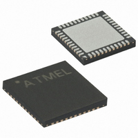
ATMEGA644V-10MU Atmel, ATMEGA644V-10MU Datasheet - Page 233

ATMEGA644V-10MU
Manufacturer Part Number
ATMEGA644V-10MU
Description
IC AVR MCU FLASH 64K 44-QFN
Manufacturer
Atmel
Series
AVR® ATmegar
Specifications of ATMEGA644V-10MU
Core Processor
AVR
Core Size
8-Bit
Speed
10MHz
Connectivity
I²C, SPI, UART/USART
Peripherals
Brown-out Detect/Reset, POR, PWM, WDT
Number Of I /o
32
Program Memory Size
64KB (32K x 16)
Program Memory Type
FLASH
Eeprom Size
2K x 8
Ram Size
4K x 8
Voltage - Supply (vcc/vdd)
1.8 V ~ 5.5 V
Data Converters
A/D 8x10b
Oscillator Type
Internal
Operating Temperature
-40°C ~ 85°C
Package / Case
44-VQFN Exposed Pad
Package
44QFN EP
Device Core
AVR
Family Name
ATmega
Maximum Speed
10 MHz
Operating Supply Voltage
2.5|3.3|5 V
Data Bus Width
8 Bit
Number Of Programmable I/os
32
Interface Type
JTAG/SPI/TWI/USART
On-chip Adc
8-chx10-bit
Number Of Timers
3
Processor Series
ATMEGA64x
Core
AVR8
Data Ram Size
4 KB
Maximum Clock Frequency
20 MHz
Maximum Operating Temperature
+ 85 C
Mounting Style
SMD/SMT
Minimum Operating Temperature
- 40 C
For Use With
ATSTK600-TQFP44 - STK600 SOCKET/ADAPTER 44-TQFPATSTK600 - DEV KIT FOR AVR/AVR32770-1007 - ISP 4PORT ATMEL AVR MCU SPI/JTAGATAVRISP2 - PROGRAMMER AVR IN SYSTEM
Lead Free Status / RoHS Status
Lead free / RoHS Compliant
Available stocks
Company
Part Number
Manufacturer
Quantity
Price
Part Number:
ATMEGA644V-10MU
Manufacturer:
ATMEL/爱特梅尔
Quantity:
20 000
- Current page: 233 of 376
- Download datasheet (8Mb)
21. Analog-to-digital Converter
21.1
21.2
2593N–AVR–07/10
Features
Overview
•
•
•
•
•
•
•
•
•
•
•
•
•
•
•
Note:
The ATmega644 features a 10-bit successive approximation ADC. The ADC is connected to an
8-channel Analog Multiplexer which allows 8 single-ended voltage inputs constructed from the
pins of Port A. The single-ended voltage inputs refer to 0V (GND).
The device also supports 16 differential voltage input combinations. Two of the differential inputs
(ADC1, ADC0 and ADC3, ADC2) are equipped with a programmable gain stage, providing
amplification steps of 0 dB (1x), 20 dB (10x), or 46 dB (200x) on the differential input voltage
before the A/D conversion. Seven differential analog input channels share a common negative
terminal (ADC1), while any other ADC input can be selected as the positive input terminal. If 1x
or 10× gain is used, 8-bit resolution can be expected. If 200x gain is used, 7-bit resolution can be
expected.
The ADC contains a Sample and Hold circuit which ensures that the input voltage to the ADC is
held at a constant level during conversion. A block diagram of the ADC is shown in
The ADC has a separate analog supply voltage pin, AVCC. AVCC must not differ more than
±0.3V from V
pin.
Internal reference voltages of nominally 1.1V, 2.56V or AVCC are provided On-chip. The voltage
reference may be externally decoupled at the AREF pin by a capacitor for better noise
performance.
10-bit Resolution
0.5 LSB Integral Non-linearity
±2 LSB Absolute Accuracy
65 µs - 260 µs Conversion Time
Up to 15 kSPS at Maximum Resolution
8 Multiplexed Single Ended Input Channels
Differential mode with selectable gain at 1x, 10x or 200x
Optional Left adjustment for ADC Result Readout
0V - V
2.7V - V
Selectable 2.56V or 1.1V ADC Reference Voltage
Free Running or Single Conversion Mode
ADC Start Conversion by Auto Triggering on Interrupt Sources
Interrupt on ADC Conversion Complete
Sleep Mode Noise Canceler
CC
1. The differential input channels are not tested for devices in PDIP Package. This feature is only
CC
ADC Input Voltage Range
guaranteed to work for devices in TQFP and QFN/MLF Packages.
Differential ADC Voltage Range
CC
. See the paragraph
”ADC Noise Canceler” on page 241
on how to connect this
ATmega644
Figure
21-1.
233
Related parts for ATMEGA644V-10MU
Image
Part Number
Description
Manufacturer
Datasheet
Request
R

Part Number:
Description:
Manufacturer:
Atmel Corporation
Datasheet:

Part Number:
Description:
IC AVR MCU FLASH 64K 44-QFN
Manufacturer:
Atmel
Datasheet:

Part Number:
Description:
IC AVR MCU FLASH 64K 44TQFP
Manufacturer:
Atmel
Datasheet:

Part Number:
Description:
IC AVR MCU FLASH 64K 40DIP
Manufacturer:
Atmel
Datasheet:

Part Number:
Description:
MCU AVR 64K FLASH 20MHZ 44TQFP
Manufacturer:
Atmel
Datasheet:

Part Number:
Description:
MCU AVR 64K FLASH 20MHZ 44QFN
Manufacturer:
Atmel
Datasheet:

Part Number:
Description:
Atmega644 8-bit Avr Microcontroller With 64k Bytes In-system Programmable Flash
Manufacturer:
ATMEL Corporation
Datasheet:

Part Number:
Description:
Manufacturer:
Atmel Corporation
Datasheet:

Part Number:
Description:
Manufacturer:
ATMEL Corporation
Datasheet:

Part Number:
Description:
Manufacturer:
ATMEL Corporation
Datasheet:

Part Number:
Description:
IC AVR MCU 64K 16MHZ 5V 64TQFP
Manufacturer:
Atmel
Datasheet:

Part Number:
Description:
IC AVR MCU 64K 16MHZ 5V 64-QFN
Manufacturer:
Atmel
Datasheet:


