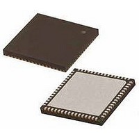
PIC18F65K22-I/MRRSL Microchip Technology, PIC18F65K22-I/MRRSL Datasheet - Page 293

PIC18F65K22-I/MRRSL
Manufacturer Part Number
PIC18F65K22-I/MRRSL
Description
MCU PIC 32K FLASH MEM XLP 64QFN
Manufacturer
Microchip Technology
Series
PIC® XLP™ 18Fr
Datasheets
1.PIC16F722-ISS.pdf
(8 pages)
2.PIC18F65K22T-IPTRSL.pdf
(548 pages)
3.PIC18F65K22T-IPTRSL.pdf
(10 pages)
Specifications of PIC18F65K22-I/MRRSL
Core Size
8-Bit
Program Memory Size
32KB (16K x 16)
Core Processor
PIC
Speed
64MHz
Connectivity
I²C, LIN, SPI, UART/USART
Peripherals
Brown-out Detect/Reset, LVD, POR, PWM, WDT
Number Of I /o
53
Program Memory Type
FLASH
Eeprom Size
1K x 8
Ram Size
2K x 8
Voltage - Supply (vcc/vdd)
1.8 V ~ 5.5 V
Data Converters
A/D 16x12b
Oscillator Type
Internal
Operating Temperature
-40°C ~ 85°C
Package / Case
64-VFQFN, Exposed Pad
Controller Family/series
PIC18
No. Of I/o's
53
Eeprom Memory Size
1KB
Ram Memory Size
2KB
Cpu Speed
64MHz
No. Of Timers
8
Processor Series
PIC18F
Core
PIC
Data Bus Width
8 bit
Data Ram Size
2 KB
Interface Type
I2C, SPI
Maximum Clock Frequency
64 MHz
Number Of Programmable I/os
53
Number Of Timers
8
Operating Supply Voltage
1.8 V to 5.5 V
Maximum Operating Temperature
+ 125 C
Mounting Style
SMD/SMT
3rd Party Development Tools
52715-96, 52716-328, 52717-734, 52712-325, EWPIC18
Minimum Operating Temperature
- 40 C
On-chip Adc
12 bit, 16 Channel
Lead Free Status / RoHS Status
Lead free / RoHS Compliant
Lead Free Status / RoHS Status
Lead free / RoHS Compliant
- PIC16F722-ISS PDF datasheet
- PIC18F65K22T-IPTRSL PDF datasheet #2
- PIC18F65K22T-IPTRSL PDF datasheet #3
- Current page: 293 of 548
- Download datasheet (5Mb)
REGISTER 21-6:
REGISTER 21-7:
2010 Microchip Technology Inc.
bit 7
Legend:
R = Readable bit
-n = Value at POR
bit 7
bit 6
bit 5
bit 4
bit 3
bit 2
bit 1
bit 0
Note 1:
bit 7
Legend:
R = Readable bit
-n = Value at POR
bit 7-0
Note 1:
R/W-0
GCEN
R/W-1
MSK7
2:
If the I
writes to the SSPxBUF are disabled).
This register shares the same SFR address as SSPxADD and is only addressable in select MSSPx
operating modes. See Section 21.4.3.4 “7-Bit Address Masking Mode” for more details.
MSK0 is not used as a mask bit in 7-bit addressing.
GCEN: General Call Enable bit
1 = Enables interrupt when a general call address (0000h) is received in the SSPxSR
0 = General call address is disabled
ACKSTAT: Acknowledge Status bit
Unused in Slave mode.
ACKDT: Acknowledge Data bit (Master Receive mode only)
1 = Not Acknowledge
0 = Acknowledge
ACKEN: Acknowledge Sequence Enable bit
1 = Initiates Acknowledge sequence on SDAx and SCLx pins and transmits ACKDT data bit.
0 = Acknowledge sequence is Idle
RCEN: Receive Enable bit (Master Receive mode only)
1 = Enables Receive mode for I
0 = Receive is Idle
PEN: Stop Condition Enable bit
1 = Initiates Stop condition on SDAx and SCLx pins. Automatically cleared by hardware.
0 = Stop condition is Idle
RSEN: Repeated Start Condition Enable bit
1 = Initiates Repeated Start condition on SDAx and SCLx pins. Automatically cleared by hardware.
0 = Repeated Start condition is Idle
SEN: Stretch Enable bit
1 = Clock stretching is enabled for both slave transmit and slave receive (stretch enabled)
0 = Clock stretching is disabled
MSK<7:0>: Slave Address Mask Select bit
1 = Masking of corresponding bit of SSPxADD is enabled
0 = Masking of corresponding bit of SSPxADD is disabled
ACKSTAT
2
R/W-1
C module is active, this bit may not be set (no spooling) and the SSPxBUF may not be written (or
R/W-1
MSK6
Automatically cleared by hardware.
SSPxCON2: MSSPx CONTROL REGISTER 2 (I
SSPxMSK: I
W = Writable bit
‘1’ = Bit is set
W = Writable bit
‘1’ = Bit is set
ACKDT
R/W-0
R/W-1
MSK5
2
C™ SLAVE ADDRESS MASK REGISTER (7-BIT MASKING MODE)
(1)
ACKEN
(1)
2
C™
R/W-0
R/W-1
MSK4
Preliminary
(1)
(1)
U = Unimplemented bit, read as ‘0’
‘0’ = Bit is cleared
U = Unimplemented bit, read as ‘0’
‘0’ = Bit is cleared
(1)
PIC18F87K22 FAMILY
RCEN
R/W-0
R/W-1
MSK3
(1)
(1)
(1)
2
PEN
R/W-0
R/W-1
MSK2
C™ SLAVE MODE)
(1)
x = Bit is unknown
x = Bit is unknown
RSEN
R/W-0
R/W-1
MSK1
(1)
DS39960B-page 293
MSK0
SEN
R/W-0
R/W-1
(1)
(2)
bit 0
bit 0
(1)
Related parts for PIC18F65K22-I/MRRSL
Image
Part Number
Description
Manufacturer
Datasheet
Request
R

Part Number:
Description:
MCU PIC 32K FLASH MEM XLP 64TQFP
Manufacturer:
Microchip Technology
Datasheet:

Part Number:
Description:
32kB Flash, 2kB RAM, 1kB EE, NanoWatt XLP, GP 64 QFN 9x9x0.9mm TUBE
Manufacturer:
Microchip Technology
Datasheet:

Part Number:
Description:
32kB Flash, 2kB RAM, 1kB EE, NanoWatt XLP, GP 64 TQFP 10x10x1mm TRAY
Manufacturer:
Microchip Technology
Datasheet:

Part Number:
Description:
32kB Flash, 2kB RAM, 1kB EE, NanoWatt XLP, GP 64 QFN 9x9x0.9mm TUBE
Manufacturer:
Microchip Technology
Datasheet:

Part Number:
Description:
32kB Flash, 2kB RAM, 1kB EE, NanoWatt XLP, GP 64 TQFP 10x10x1mm TRAY
Manufacturer:
Microchip Technology

Part Number:
Description:
Manufacturer:
Microchip Technology Inc.
Datasheet:

Part Number:
Description:
Manufacturer:
Microchip Technology Inc.
Datasheet:

Part Number:
Description:
Manufacturer:
Microchip Technology Inc.
Datasheet:

Part Number:
Description:
Manufacturer:
Microchip Technology Inc.
Datasheet:

Part Number:
Description:
Manufacturer:
Microchip Technology Inc.
Datasheet:

Part Number:
Description:
Manufacturer:
Microchip Technology Inc.
Datasheet:


