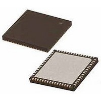
PIC18F65K22-I/MRRSL Microchip Technology, PIC18F65K22-I/MRRSL Datasheet - Page 251

PIC18F65K22-I/MRRSL
Manufacturer Part Number
PIC18F65K22-I/MRRSL
Description
MCU PIC 32K FLASH MEM XLP 64QFN
Manufacturer
Microchip Technology
Series
PIC® XLP™ 18Fr
Datasheets
1.PIC16F722-ISS.pdf
(8 pages)
2.PIC18F65K22T-IPTRSL.pdf
(548 pages)
3.PIC18F65K22T-IPTRSL.pdf
(10 pages)
Specifications of PIC18F65K22-I/MRRSL
Core Size
8-Bit
Program Memory Size
32KB (16K x 16)
Core Processor
PIC
Speed
64MHz
Connectivity
I²C, LIN, SPI, UART/USART
Peripherals
Brown-out Detect/Reset, LVD, POR, PWM, WDT
Number Of I /o
53
Program Memory Type
FLASH
Eeprom Size
1K x 8
Ram Size
2K x 8
Voltage - Supply (vcc/vdd)
1.8 V ~ 5.5 V
Data Converters
A/D 16x12b
Oscillator Type
Internal
Operating Temperature
-40°C ~ 85°C
Package / Case
64-VFQFN, Exposed Pad
Controller Family/series
PIC18
No. Of I/o's
53
Eeprom Memory Size
1KB
Ram Memory Size
2KB
Cpu Speed
64MHz
No. Of Timers
8
Processor Series
PIC18F
Core
PIC
Data Bus Width
8 bit
Data Ram Size
2 KB
Interface Type
I2C, SPI
Maximum Clock Frequency
64 MHz
Number Of Programmable I/os
53
Number Of Timers
8
Operating Supply Voltage
1.8 V to 5.5 V
Maximum Operating Temperature
+ 125 C
Mounting Style
SMD/SMT
3rd Party Development Tools
52715-96, 52716-328, 52717-734, 52712-325, EWPIC18
Minimum Operating Temperature
- 40 C
On-chip Adc
12 bit, 16 Channel
Lead Free Status / RoHS Status
Lead free / RoHS Compliant
Lead Free Status / RoHS Status
Lead free / RoHS Compliant
- PIC16F722-ISS PDF datasheet
- PIC18F65K22T-IPTRSL PDF datasheet #2
- PIC18F65K22T-IPTRSL PDF datasheet #3
- Current page: 251 of 548
- Download datasheet (5Mb)
FIGURE 19-2:
TABLE 19-5:
2010 Microchip Technology Inc.
INTCON
RCON
PIR4
PIE4
IPR4
TRISB
TRISC
TRISE
TRISH
TMR1L
Legend: — = unimplemented, read as ‘0’. Shaded cells are not used by Capture/Compare or Timer1/3/5/7.
Note 1:
Name
2:
(2)
Note:
Unimplemented on devices with a program memory of 32 Kbytes (PIC18F65K22 and PIC18F85K22).
Unimplemented on 64-pin devices (PIC18F65K22, PIC18F66K22 and PIC18F67K22).
1
0
CCP10IE
CCP10IP
Timer1 Register Low Byte
CCP10IF
CCPR5H
GIE/GIEH PEIE/GIEL
TMR1H
TMR5H
This block diagram uses CCP4 and CCP5 and their appropriate timers as an example. For details on all of
the CCP modules and their timer assignments, see Table 19-2 and Table 19-3.
TRISB7
TRISC7
TRISE7
TRISH7
REGISTERS ASSOCIATED WITH CAPTURE, COMPARE, TIMER1/3/5/7
IPEN
Bit 7
Comparator
COMPARE MODE OPERATION BLOCK DIAGRAM
CCPR4H
TMR1H
TMR5H
(1)
(1)
(1)
C4TSEL0
C4TSEL1
CCPR5L
TMR1L
Comparator
TMR5L
CCP9IE
CCP9IP
CCP9IF
SBOREN
TRISB6
TRISC6
TRISE6
TRISH6
Bit 6
CCPR4L
TMR1L
TMR5L
Compare
C5TSEL0
Match
(1)
(1)
(1)
0
1
Set CCP5IF
Compare
TMR0IE
CCP8IE
CCP8IP
CCP8IF
TRISB5
TRISC5
TRISE5
TRISH5
Match
Bit 5
CM
Preliminary
Set CCP4IF
CCP7IE
CCP7IP
CCP7IF
TRISB4
TRISC4
TRISE4
TRISH4
INT0IE
Bit 4
Special Event Trigger
RI
CCP5CON<3:0>
(Timer1/Timer3 Reset, A/D Trigger)
(Timer1/5 Reset)
PIC18F87K22 FAMILY
Output
Logic
4
Special Event Trigger
CCP4CON<3:0>
CCP6IE
CCP6IP
CCP6IF
TRISB3
TRISC3
TRISE3
TRISH3
Output
RBIE
Bit 3
Logic
4
TO
S
R
Q
TMR0IF
CCP5IE
CCP5IP
CCP5IF
TRISB2
TRISC2
TRISE2
TRISH2
S
R
Bit 2
PD
Output Enable
Q
TRIS
Output Enable
CCP4IE
CCP4IP
CCP4IF
TRISB1
TRISC1
TRISE1
TRISH1
CCP5 Pin
INT0IF
TRIS
Bit 1
POR
DS39960B-page 251
CCP4 Pin
CCP3IF
CCP3IE
CCP3IP
TRISB0
TRISC0
TRISE0
TRISH0
RBIF
Bit 0
BOR
Related parts for PIC18F65K22-I/MRRSL
Image
Part Number
Description
Manufacturer
Datasheet
Request
R

Part Number:
Description:
MCU PIC 32K FLASH MEM XLP 64TQFP
Manufacturer:
Microchip Technology
Datasheet:

Part Number:
Description:
32kB Flash, 2kB RAM, 1kB EE, NanoWatt XLP, GP 64 QFN 9x9x0.9mm TUBE
Manufacturer:
Microchip Technology
Datasheet:

Part Number:
Description:
32kB Flash, 2kB RAM, 1kB EE, NanoWatt XLP, GP 64 TQFP 10x10x1mm TRAY
Manufacturer:
Microchip Technology
Datasheet:

Part Number:
Description:
32kB Flash, 2kB RAM, 1kB EE, NanoWatt XLP, GP 64 QFN 9x9x0.9mm TUBE
Manufacturer:
Microchip Technology
Datasheet:

Part Number:
Description:
32kB Flash, 2kB RAM, 1kB EE, NanoWatt XLP, GP 64 TQFP 10x10x1mm TRAY
Manufacturer:
Microchip Technology

Part Number:
Description:
Manufacturer:
Microchip Technology Inc.
Datasheet:

Part Number:
Description:
Manufacturer:
Microchip Technology Inc.
Datasheet:

Part Number:
Description:
Manufacturer:
Microchip Technology Inc.
Datasheet:

Part Number:
Description:
Manufacturer:
Microchip Technology Inc.
Datasheet:

Part Number:
Description:
Manufacturer:
Microchip Technology Inc.
Datasheet:

Part Number:
Description:
Manufacturer:
Microchip Technology Inc.
Datasheet:


