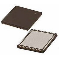
PIC18F65K22-I/MRRSL Microchip Technology, PIC18F65K22-I/MRRSL Datasheet - Page 280

PIC18F65K22-I/MRRSL
Manufacturer Part Number
PIC18F65K22-I/MRRSL
Description
MCU PIC 32K FLASH MEM XLP 64QFN
Manufacturer
Microchip Technology
Series
PIC® XLP™ 18Fr
Datasheets
1.PIC16F722-ISS.pdf
(8 pages)
2.PIC18F65K22T-IPTRSL.pdf
(548 pages)
3.PIC18F65K22T-IPTRSL.pdf
(10 pages)
Specifications of PIC18F65K22-I/MRRSL
Core Size
8-Bit
Program Memory Size
32KB (16K x 16)
Core Processor
PIC
Speed
64MHz
Connectivity
I²C, LIN, SPI, UART/USART
Peripherals
Brown-out Detect/Reset, LVD, POR, PWM, WDT
Number Of I /o
53
Program Memory Type
FLASH
Eeprom Size
1K x 8
Ram Size
2K x 8
Voltage - Supply (vcc/vdd)
1.8 V ~ 5.5 V
Data Converters
A/D 16x12b
Oscillator Type
Internal
Operating Temperature
-40°C ~ 85°C
Package / Case
64-VFQFN, Exposed Pad
Controller Family/series
PIC18
No. Of I/o's
53
Eeprom Memory Size
1KB
Ram Memory Size
2KB
Cpu Speed
64MHz
No. Of Timers
8
Processor Series
PIC18F
Core
PIC
Data Bus Width
8 bit
Data Ram Size
2 KB
Interface Type
I2C, SPI
Maximum Clock Frequency
64 MHz
Number Of Programmable I/os
53
Number Of Timers
8
Operating Supply Voltage
1.8 V to 5.5 V
Maximum Operating Temperature
+ 125 C
Mounting Style
SMD/SMT
3rd Party Development Tools
52715-96, 52716-328, 52717-734, 52712-325, EWPIC18
Minimum Operating Temperature
- 40 C
On-chip Adc
12 bit, 16 Channel
Lead Free Status / RoHS Status
Lead free / RoHS Compliant
Lead Free Status / RoHS Status
Lead free / RoHS Compliant
- PIC16F722-ISS PDF datasheet
- PIC18F65K22T-IPTRSL PDF datasheet #2
- PIC18F65K22T-IPTRSL PDF datasheet #3
- Current page: 280 of 548
- Download datasheet (5Mb)
PIC18F87K22 FAMILY
21.3.1
Each MSSP module has four registers for SPI mode
operation. These are:
• MSSPx Control Register 1 (SSPxCON1)
• MSSPx Status Register (SSPxSTAT)
• Serial Receive/Transmit Buffer Register
• MSSPx Shift Register (SSPxSR) – Not directly
SSPxCON1 and SSPxSTAT are the control and status
registers in SPI mode operation. The SSPxCON1
register is readable and writable. The lower 6 bits of
the SSPxSTAT are read-only. The upper two bits of the
SSPxSTAT are read/write.
REGISTER 21-1:
DS39960B-page 280
bit 7
Legend:
R = Readable bit
-n = Value at POR
bit 7
bit 6
bit 5
bit 4
bit 3
bit 2
bit 1
bit 0
Note 1:
(SSPxBUF)
accessible
R/W-0
SMP
Polarity of clock state is set by the CKP bit (SSPxCON1<4>).
REGISTERS
SMP: Sample bit
SPI Master mode:
1 = Input data sampled at the end of data output time
0 = Input data sampled at the middle of data output time
SPI Slave mode:
SMP must be cleared when SPI is used in Slave mode.
CKE: SPI Clock Select bit
1 = Transmit occurs on the transition from active to Idle clock state
0 = Transmit occurs on the transition from Idle to active clock state
D/A: Data/Address bit
Used in I
P: Stop bit
Used in I
S: Start bit
Used in I
R/W: Read/Write Information bit
Used in I
UA: Update Address bit
Used in I
BF: Buffer Full Status bit (Receive mode only)
1 = Receive is complete, SSPxBUF is full
0 = Receive is not complete, SSPxBUF is empty
CKE
R/W-0
SSPxSTAT: MSSPx STATUS REGISTER (SPI MODE)
(1)
2
2
2
2
2
C™ mode only.
C mode only. This bit is cleared when the MSSPx module is disabled; SSPEN is cleared.
C mode only.
C mode only.
C mode only.
W = Writable bit
‘1’ = Bit is set
R-0
D/A
(1)
R-0
Preliminary
P
U = Unimplemented bit, read as ‘0’
‘0’ = Bit is cleared
SSPxSR is the shift register used for shifting data in or
out. SSPxBUF is the buffer register to which data
bytes are written to or read from.
In receive operations, SSPxSR and SSPxBUF
together create a double-buffered receiver. When
SSPxSR receives a complete byte, it is transferred to
SSPxBUF and the SSPxIF interrupt is set.
During
double-buffered. A write to SSPxBUF will write to both
SSPxBUF and SSPxSR.
R-0
S
transmission,
R/W
R-0
2010 Microchip Technology Inc.
x = Bit is unknown
the
R-0
UA
SSPxBUF
R-0
BF
is
bit 0
not
Related parts for PIC18F65K22-I/MRRSL
Image
Part Number
Description
Manufacturer
Datasheet
Request
R

Part Number:
Description:
MCU PIC 32K FLASH MEM XLP 64TQFP
Manufacturer:
Microchip Technology
Datasheet:

Part Number:
Description:
32kB Flash, 2kB RAM, 1kB EE, NanoWatt XLP, GP 64 QFN 9x9x0.9mm TUBE
Manufacturer:
Microchip Technology
Datasheet:

Part Number:
Description:
32kB Flash, 2kB RAM, 1kB EE, NanoWatt XLP, GP 64 TQFP 10x10x1mm TRAY
Manufacturer:
Microchip Technology
Datasheet:

Part Number:
Description:
32kB Flash, 2kB RAM, 1kB EE, NanoWatt XLP, GP 64 QFN 9x9x0.9mm TUBE
Manufacturer:
Microchip Technology
Datasheet:

Part Number:
Description:
32kB Flash, 2kB RAM, 1kB EE, NanoWatt XLP, GP 64 TQFP 10x10x1mm TRAY
Manufacturer:
Microchip Technology

Part Number:
Description:
Manufacturer:
Microchip Technology Inc.
Datasheet:

Part Number:
Description:
Manufacturer:
Microchip Technology Inc.
Datasheet:

Part Number:
Description:
Manufacturer:
Microchip Technology Inc.
Datasheet:

Part Number:
Description:
Manufacturer:
Microchip Technology Inc.
Datasheet:

Part Number:
Description:
Manufacturer:
Microchip Technology Inc.
Datasheet:

Part Number:
Description:
Manufacturer:
Microchip Technology Inc.
Datasheet:


