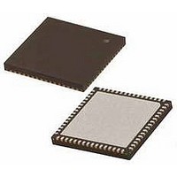
PIC18F65K22-I/MRRSL Microchip Technology, PIC18F65K22-I/MRRSL Datasheet - Page 213

PIC18F65K22-I/MRRSL
Manufacturer Part Number
PIC18F65K22-I/MRRSL
Description
MCU PIC 32K FLASH MEM XLP 64QFN
Manufacturer
Microchip Technology
Series
PIC® XLP™ 18Fr
Datasheets
1.PIC16F722-ISS.pdf
(8 pages)
2.PIC18F65K22T-IPTRSL.pdf
(548 pages)
3.PIC18F65K22T-IPTRSL.pdf
(10 pages)
Specifications of PIC18F65K22-I/MRRSL
Core Size
8-Bit
Program Memory Size
32KB (16K x 16)
Core Processor
PIC
Speed
64MHz
Connectivity
I²C, LIN, SPI, UART/USART
Peripherals
Brown-out Detect/Reset, LVD, POR, PWM, WDT
Number Of I /o
53
Program Memory Type
FLASH
Eeprom Size
1K x 8
Ram Size
2K x 8
Voltage - Supply (vcc/vdd)
1.8 V ~ 5.5 V
Data Converters
A/D 16x12b
Oscillator Type
Internal
Operating Temperature
-40°C ~ 85°C
Package / Case
64-VFQFN, Exposed Pad
Controller Family/series
PIC18
No. Of I/o's
53
Eeprom Memory Size
1KB
Ram Memory Size
2KB
Cpu Speed
64MHz
No. Of Timers
8
Processor Series
PIC18F
Core
PIC
Data Bus Width
8 bit
Data Ram Size
2 KB
Interface Type
I2C, SPI
Maximum Clock Frequency
64 MHz
Number Of Programmable I/os
53
Number Of Timers
8
Operating Supply Voltage
1.8 V to 5.5 V
Maximum Operating Temperature
+ 125 C
Mounting Style
SMD/SMT
3rd Party Development Tools
52715-96, 52716-328, 52717-734, 52712-325, EWPIC18
Minimum Operating Temperature
- 40 C
On-chip Adc
12 bit, 16 Channel
Lead Free Status / RoHS Status
Lead free / RoHS Compliant
Lead Free Status / RoHS Status
Lead free / RoHS Compliant
- PIC16F722-ISS PDF datasheet
- PIC18F65K22T-IPTRSL PDF datasheet #2
- PIC18F65K22T-IPTRSL PDF datasheet #3
- Current page: 213 of 548
- Download datasheet (5Mb)
16.2
Timer3, Timer5 and Timer7 can operate in these
modes:
• Timer
• Synchronous Counter
• Asynchronous Counter
• Timer with Gated Control
FIGURE 16-1:
2010 Microchip Technology Inc.
T1CON.SOSCEN
T3CON.SOSCEN
SCS<1:0> = 01
T3G
From TMR4
Match PR4
From Comparator 1
Output
From Comparator 2
Output
Timer3/5/7 Operation
Note 1:
T3GSS<1:0>
SOSCGO
SOSCO/SCLKI
2:
3:
4:
T3GPOL
SOSCI
T3CKI
ST Buffer is high-speed type when using T3CKI.
Timer3 registers increment on rising edge.
Synchronization does not operate while in Sleep.
The output of SOSC is determined by the SOSCSEL<1:0> Configuration bits.
Set flag bit
TMR3IF on
Overflow
Timer3/5/7 BLOCK DIAGRAM
00
10
11
01
TMR3ON
T3GTM
TMR3H
SOSC
EN
OUT
TMR3
(1)
T3G_IN
(4)
(2)
D
R
CK
TMR3L
Q
Q
1
0
Preliminary
TMR3CS<1:0>
0
1
T3GGO/T3DONE
Q
Internal
Internal
F
OSC
Clock
Clock
F
PIC18F87K22 FAMILY
OSC
EN
/4
The operating mode is determined by the clock select
bits, TMRxCSx (TxCON<7:6>). When the TMRxCSx bits
are cleared (= 00), Timer3/5/7 increments on every inter-
nal instruction cycle (F
Timer3/5/7 clock source is the system clock (F
when it is ‘10’, Timer3/5/7 works as a counter from the
external clock from the TxCKI pin (on the rising edge after
the first falling edge) or the SOSC oscillator.
D
Single Pulse
Acq. Control
10
01
00
T3CLK
T3GSPM
T3CKPS<1:0>
T3SYNC
Prescaler
1, 2, 4, 8
TMR3ON
0
1
2
0
1
Internal
F
OSC
Clock
T3GVAL
OSC
TMR3GE
/2
/4). When TMRxCSx = 01, the
Q1
Synchronized
Synchronize
Interrupt
Clock Input
D
EN
det
det
Sleep Input
Q
DS39960B-page 213
(3)
Set
TMR3GIF
T3GCON
Data Bus
OSC
RD
), and
Related parts for PIC18F65K22-I/MRRSL
Image
Part Number
Description
Manufacturer
Datasheet
Request
R

Part Number:
Description:
MCU PIC 32K FLASH MEM XLP 64TQFP
Manufacturer:
Microchip Technology
Datasheet:

Part Number:
Description:
32kB Flash, 2kB RAM, 1kB EE, NanoWatt XLP, GP 64 QFN 9x9x0.9mm TUBE
Manufacturer:
Microchip Technology
Datasheet:

Part Number:
Description:
32kB Flash, 2kB RAM, 1kB EE, NanoWatt XLP, GP 64 TQFP 10x10x1mm TRAY
Manufacturer:
Microchip Technology
Datasheet:

Part Number:
Description:
32kB Flash, 2kB RAM, 1kB EE, NanoWatt XLP, GP 64 QFN 9x9x0.9mm TUBE
Manufacturer:
Microchip Technology
Datasheet:

Part Number:
Description:
32kB Flash, 2kB RAM, 1kB EE, NanoWatt XLP, GP 64 TQFP 10x10x1mm TRAY
Manufacturer:
Microchip Technology

Part Number:
Description:
Manufacturer:
Microchip Technology Inc.
Datasheet:

Part Number:
Description:
Manufacturer:
Microchip Technology Inc.
Datasheet:

Part Number:
Description:
Manufacturer:
Microchip Technology Inc.
Datasheet:

Part Number:
Description:
Manufacturer:
Microchip Technology Inc.
Datasheet:

Part Number:
Description:
Manufacturer:
Microchip Technology Inc.
Datasheet:

Part Number:
Description:
Manufacturer:
Microchip Technology Inc.
Datasheet:


