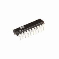
ATTINY26-16PU Atmel, ATTINY26-16PU Datasheet - Page 75

ATTINY26-16PU
Manufacturer Part Number
ATTINY26-16PU
Description
IC AVR MCU 2K 16MHZ IND 20-DIP
Manufacturer
Atmel
Series
AVR® ATtinyr
Specifications of ATTINY26-16PU
Core Processor
AVR
Core Size
8-Bit
Speed
16MHz
Connectivity
USI
Peripherals
Brown-out Detect/Reset, POR, PWM, WDT
Number Of I /o
16
Program Memory Size
2KB (1K x 16)
Program Memory Type
FLASH
Eeprom Size
128 x 8
Ram Size
128 x 8
Voltage - Supply (vcc/vdd)
4.5 V ~ 5.5 V
Data Converters
A/D 11x10b
Oscillator Type
Internal
Operating Temperature
-40°C ~ 85°C
Package / Case
20-DIP (0.300", 7.62mm)
Processor Series
ATTINY2x
Core
AVR8
Data Bus Width
8 bit
Data Ram Size
128 B
Interface Type
2-Wire/ISP/SM-Bus/SPI/UART/USI
Maximum Clock Frequency
16 MHz
Number Of Programmable I/os
16
Number Of Timers
2
Operating Supply Voltage
4.5 V to 5.5 V
Maximum Operating Temperature
+ 85 C
Mounting Style
Through Hole
3rd Party Development Tools
EWAVR, EWAVR-BL
Development Tools By Supplier
ATAVRDRAGON, ATSTK500, ATSTK600, ATAVRISP2, ATAVRONEKIT
Minimum Operating Temperature
- 40 C
On-chip Adc
11-ch x 10-bit
Package
20PDIP
Device Core
AVR
Family Name
ATtiny
Maximum Speed
16 MHz
For Use With
ATSTK600 - DEV KIT FOR AVR/AVR32770-1007 - ISP 4PORT ATMEL AVR MCU SPI/JTAGATAVRISP2 - PROGRAMMER AVR IN SYSTEMATSTK505 - ADAPTER KIT FOR 14PIN AVR MCU
Lead Free Status / RoHS Status
Lead free / RoHS Compliant
- Current page: 75 of 182
- Download datasheet (3Mb)
1477K–AVR–08/10
Table 35. Compare Mode Select in PWM Mode
Note that in PWM mode, writing to the Output Compare Registers OCR1A or OCR1B, the data
value is first transferred to a temporary location. The value is latched into OCR1A or OCR1B
when the Timer/Counter reaches OCR1C. This prevents the occurrence of odd-length PWM
pulses (glitches) in the event of an unsynchronized OCR1A or OCR1B. See Figure 42 for an
example.
Figure 42. Effects of Unsynchronized OCR Latching
During the time between the write and the latch operation, a read from OCR1A or OCR1B will
read the contents of the temporary location. This means that the most recently written value
always will read out of OCR1A or OCR1B.
When OCR1A or OCR1B contain $00 or the top value, as specified in OCR1C Register, the out-
p u t P B 1 ( O C 1 A ) o r P B 3 ( O C 1 B ) i s h e l d l o w o r h i g h a c c o r d i n g t o t h e s e t t i n g s o f
COM1A1/COM1A0. This is shown in Table 36.
COM1x1
0
0
1
1
Unsynchronized OC1x Latch
Synchronized OC1x Latch
COM1x0
0
1
0
1
Effect on Output Compare Pins
OC1x not connected.
OC1x not connected.
OC1x cleared on compare match. Set when TCNT1 = $01.
OC1x set one prescaled cycle after compare match. Cleared when
TCNT1 = $00.
OC1x cleared on compare match. Set when TCNT1 = $01.
OC1x not connected.
OC1x set one prescaled cycle after compare match. Cleared when
TCNT = $00
OC1x not connected.
Glitch
Compare Value changes
Compare Value Changes
Counter Value
Compare Value
PWM Output OC1x
Counter Value
Compare Value
PWM Output OC1x
75
Related parts for ATTINY26-16PU
Image
Part Number
Description
Manufacturer
Datasheet
Request
R

Part Number:
Description:
Manufacturer:
Atmel Corporation
Datasheet:

Part Number:
Description:
IC AVR MCU 2K 16MHZ IND 32-QFN
Manufacturer:
Atmel
Datasheet:

Part Number:
Description:
IC AVR MCU 2K 16MHZ IND 20-SOIC
Manufacturer:
Atmel
Datasheet:

Part Number:
Description:
IC AVR MCU 2K 16MHZ IND 32-QFN
Manufacturer:
Atmel
Datasheet:

Part Number:
Description:
IC AVR MCU 2K 16MHZ IND 20-DIP
Manufacturer:
Atmel
Datasheet:

Part Number:
Description:
IC AVR MCU 2K 16MHZ COM 20-SOIC
Manufacturer:
Atmel
Datasheet:

Part Number:
Description:
IC AVR MCU 2K 16MHZ IND 20-SOIC
Manufacturer:
Atmel
Datasheet:

Part Number:
Description:
ID MCU AVR 2K 5V 16MHZ 32-QFN
Manufacturer:
Atmel
Datasheet:

Part Number:
Description:
Microcontrollers (MCU) AVR 2K FLASH 128B EE 128B SRAM ADC
Manufacturer:
Atmel
Datasheet:

Part Number:
Description:
IC AVR MCU 2K 16MHZ COM 32-QFN
Manufacturer:
Atmel
Datasheet:

Part Number:
Description:
IC AVR MCU 2K 16MHZ COM 20-DIP
Manufacturer:
Atmel
Datasheet:

Part Number:
Description:
ID MCU AVR 2K 5V 16MHZ 20-DIP
Manufacturer:
Atmel
Datasheet:

Part Number:
Description:
ID MCU AVR 2K 5V 16MHZ 20-SOIC
Manufacturer:
Atmel
Datasheet:

Part Number:
Description:
IC MCU AVR 2K 16MHZ IND 20SOIC
Manufacturer:
Atmel
Datasheet:


