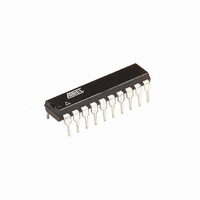
ATTINY26-16PU Atmel, ATTINY26-16PU Datasheet - Page 110

ATTINY26-16PU
Manufacturer Part Number
ATTINY26-16PU
Description
IC AVR MCU 2K 16MHZ IND 20-DIP
Manufacturer
Atmel
Series
AVR® ATtinyr
Specifications of ATTINY26-16PU
Core Processor
AVR
Core Size
8-Bit
Speed
16MHz
Connectivity
USI
Peripherals
Brown-out Detect/Reset, POR, PWM, WDT
Number Of I /o
16
Program Memory Size
2KB (1K x 16)
Program Memory Type
FLASH
Eeprom Size
128 x 8
Ram Size
128 x 8
Voltage - Supply (vcc/vdd)
4.5 V ~ 5.5 V
Data Converters
A/D 11x10b
Oscillator Type
Internal
Operating Temperature
-40°C ~ 85°C
Package / Case
20-DIP (0.300", 7.62mm)
Processor Series
ATTINY2x
Core
AVR8
Data Bus Width
8 bit
Data Ram Size
128 B
Interface Type
2-Wire/ISP/SM-Bus/SPI/UART/USI
Maximum Clock Frequency
16 MHz
Number Of Programmable I/os
16
Number Of Timers
2
Operating Supply Voltage
4.5 V to 5.5 V
Maximum Operating Temperature
+ 85 C
Mounting Style
Through Hole
3rd Party Development Tools
EWAVR, EWAVR-BL
Development Tools By Supplier
ATAVRDRAGON, ATSTK500, ATSTK600, ATAVRISP2, ATAVRONEKIT
Minimum Operating Temperature
- 40 C
On-chip Adc
11-ch x 10-bit
Package
20PDIP
Device Core
AVR
Family Name
ATtiny
Maximum Speed
16 MHz
For Use With
ATSTK600 - DEV KIT FOR AVR/AVR32770-1007 - ISP 4PORT ATMEL AVR MCU SPI/JTAGATAVRISP2 - PROGRAMMER AVR IN SYSTEMATSTK505 - ADAPTER KIT FOR 14PIN AVR MCU
Lead Free Status / RoHS Status
Lead free / RoHS Compliant
- Current page: 110 of 182
- Download datasheet (3Mb)
110
ATtiny26(L)
Figure 58. Parallel Programming
Table 54. Pin Name Mapping
Note:
Table 55. Pin Values used to Enter Programming Mode
Signal Name in
Programming Mode
WR
XA0
XA1/BS2
PAGEL/BS1
OE
RDY/BSY
DATA
Pin
PAGEL/BS1
XA1/BS2
XA0
WR
1. The pin is used for two different control signals. In the description below, normally only one of
(1)
the signals is referred. E.g., “give BS1 a positive pulse” equals “give PAGEL/BS1 a positive
pulse”.
(1)
PAGEL/BS1
RDY/BSY
XA1/BS2
Pin Name
+12 V
PA7:0
XA0
WR
PB0
PB1
PB2
PB3
PB5
PB6
OE
I/O
I/O
O
I
I
I
I
I
Prog_enable[3]
Prog_enable[2]
Prog_enable[1]
Prog_enable[0]
PB0
PB1
PB2
PB3
PB5
RESET
GND
PB6
XTAL1/PB4
Function
Write Pulse (Active low)
XTAL Action Bit 0
XTAL Action Bit 1 multiplexed with Byte Select 2
(“0” selects low byte, “1” selects 2’nd high byte)
Program Memory and EEPROM data Page Load
multiplexed with Byte Select 1 (“0” selects low
byte, “1” selects high byte).
Output Enable (Active low)
0: Device is busy programming, 1: Device is ready
for new command
Bidirectional Data bus (Output when OE is low)
Symbol
PA7: PA0
AVCC
VCC
+5V
+5V
DATA
Value
0
0
0
0
1477K–AVR–08/10
Related parts for ATTINY26-16PU
Image
Part Number
Description
Manufacturer
Datasheet
Request
R

Part Number:
Description:
Manufacturer:
Atmel Corporation
Datasheet:

Part Number:
Description:
IC AVR MCU 2K 16MHZ IND 32-QFN
Manufacturer:
Atmel
Datasheet:

Part Number:
Description:
IC AVR MCU 2K 16MHZ IND 20-SOIC
Manufacturer:
Atmel
Datasheet:

Part Number:
Description:
IC AVR MCU 2K 16MHZ IND 32-QFN
Manufacturer:
Atmel
Datasheet:

Part Number:
Description:
IC AVR MCU 2K 16MHZ IND 20-DIP
Manufacturer:
Atmel
Datasheet:

Part Number:
Description:
IC AVR MCU 2K 16MHZ COM 20-SOIC
Manufacturer:
Atmel
Datasheet:

Part Number:
Description:
IC AVR MCU 2K 16MHZ IND 20-SOIC
Manufacturer:
Atmel
Datasheet:

Part Number:
Description:
ID MCU AVR 2K 5V 16MHZ 32-QFN
Manufacturer:
Atmel
Datasheet:

Part Number:
Description:
Microcontrollers (MCU) AVR 2K FLASH 128B EE 128B SRAM ADC
Manufacturer:
Atmel
Datasheet:

Part Number:
Description:
IC AVR MCU 2K 16MHZ COM 32-QFN
Manufacturer:
Atmel
Datasheet:

Part Number:
Description:
IC AVR MCU 2K 16MHZ COM 20-DIP
Manufacturer:
Atmel
Datasheet:

Part Number:
Description:
ID MCU AVR 2K 5V 16MHZ 20-DIP
Manufacturer:
Atmel
Datasheet:

Part Number:
Description:
ID MCU AVR 2K 5V 16MHZ 20-SOIC
Manufacturer:
Atmel
Datasheet:

Part Number:
Description:
IC MCU AVR 2K 16MHZ IND 20SOIC
Manufacturer:
Atmel
Datasheet:


