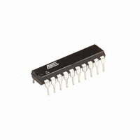
ATTINY26L-8PU Atmel, ATTINY26L-8PU Datasheet - Page 88

ATTINY26L-8PU
Manufacturer Part Number
ATTINY26L-8PU
Description
IC MCU AVR 2K 5V 8MHZ 20-DIP
Manufacturer
Atmel
Series
AVR® ATtinyr
Datasheets
1.ATTINY26-16MC.pdf
(18 pages)
2.ATTINY26-16MC.pdf
(182 pages)
3.ATTINY26L-8PU.pdf
(183 pages)
Specifications of ATTINY26L-8PU
Core Processor
AVR
Core Size
8-Bit
Speed
8MHz
Connectivity
USI
Peripherals
Brown-out Detect/Reset, POR, PWM, WDT
Number Of I /o
16
Program Memory Size
2KB (1K x 16)
Program Memory Type
FLASH
Eeprom Size
128 x 8
Ram Size
128 x 8
Voltage - Supply (vcc/vdd)
2.7 V ~ 5.5 V
Data Converters
A/D 11x10b
Oscillator Type
Internal
Operating Temperature
-40°C ~ 85°C
Package / Case
20-DIP (0.300", 7.62mm)
Processor Series
ATTINY2x
Core
AVR8
Data Bus Width
8 bit
Data Ram Size
128 B
Interface Type
2-Wire/ISP/SM-Bus/SPI/UART/USI
Maximum Clock Frequency
8 MHz
Number Of Programmable I/os
16
Number Of Timers
2
Operating Supply Voltage
2.7 V to 5.5 V
Maximum Operating Temperature
+ 85 C
Mounting Style
Through Hole
3rd Party Development Tools
EWAVR, EWAVR-BL
Development Tools By Supplier
ATAVRDRAGON, ATSTK500, ATSTK600, ATAVRISP2, ATAVRONEKIT
Minimum Operating Temperature
- 40 C
On-chip Adc
11-ch x 10-bit
Controller Family/series
AVR Tiny
No. Of I/o's
16
Eeprom Memory Size
128Byte
Ram Memory Size
128Byte
Cpu Speed
8MHz
Rohs Compliant
Yes
For Use With
ATSTK600 - DEV KIT FOR AVR/AVR32770-1007 - ISP 4PORT ATMEL AVR MCU SPI/JTAGATAVRISP2 - PROGRAMMER AVR IN SYSTEMATSTK505 - ADAPTER KIT FOR 14PIN AVR MCU
Lead Free Status / RoHS Status
Lead free / RoHS Compliant
Other names
ATTINY26L-8PJ
ATTINY26L-8PJ
ATTINY26L-8PJ
Available stocks
Company
Part Number
Manufacturer
Quantity
Price
Company:
Part Number:
ATTINY26L-8PU
Manufacturer:
Atmel
Quantity:
25 295
Part Number:
ATTINY26L-8PU
Manufacturer:
ATMEL/爱特梅尔
Quantity:
20 000
Two-wire Mode
88
ATtiny26(L)
the master device, and when the transfer is completed the data received from the mas-
ter is stored back into the r16 register.
Note that the first two instructions is for initialization only and needs only to be executed
once.These instructions sets Three-wire mode and positive edge Shift Register clock.
The loop is repeated until the USI Counter Overflow Flag is set.
The USI Two-wire mode is compliant to the Inter IC (TWI) bus protocol, but without slew
rate limiting on outputs and input noise filtering. Pin names used by this mode are SCL
and SDA.
Figure 47. Two-wire Mode Operation, Simplified Diagram
Figure 47 shows two USI units operating in Two-wire mode, one as master and one as
slave. It is only the physical layer that is shown since the system operation is highly
dependent of the communication scheme used. The main differences between the mas-
ter and slave operation at this level, is the serial clock generation which is always done
by the master, and only the slave uses the clock control unit. Clock generation must be
implemented in software, but the shift operation is done automatically by both devices.
Note that only clocking on negative edge for shifting data is of practical use in this mode.
The slave can insert wait states at start or end of transfer by forcing the SCL clock low.
This means that the master must always check if the SCL line was actually released
after it has generated a positive edge.
Since the clock also increments the counter, a counter overflow can be used to indicate
that the transfer is completed. The clock is generated by the master by toggling the PB2
pin via the PORTB Register.
The data direction is not given by the physical layer. A protocol, like the one used by the
TWI-bus, must be implemented to control the data flow.
SLAVE
MASTER
Bit7
Bit7
Bit6
Bit6
Bit5
Bit5
Bit4
Bit4
Bit3
Bit3
Bit2
Bit2
Bit1
Bit1
Bit0
Bit0
Two-wire Clock
Control Unit
PORTBz
HOLD
SCL
PBy
PBz
PBy
PBz
SDA
SCL
SDA
SCL
1477F–AVR–12/04
VCC


