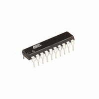
ATTINY26L-8PU Atmel, ATTINY26L-8PU Datasheet - Page 122

ATTINY26L-8PU
Manufacturer Part Number
ATTINY26L-8PU
Description
IC MCU AVR 2K 5V 8MHZ 20-DIP
Manufacturer
Atmel
Series
AVR® ATtinyr
Datasheets
1.ATTINY26-16MC.pdf
(18 pages)
2.ATTINY26-16MC.pdf
(182 pages)
3.ATTINY26L-8PU.pdf
(183 pages)
Specifications of ATTINY26L-8PU
Core Processor
AVR
Core Size
8-Bit
Speed
8MHz
Connectivity
USI
Peripherals
Brown-out Detect/Reset, POR, PWM, WDT
Number Of I /o
16
Program Memory Size
2KB (1K x 16)
Program Memory Type
FLASH
Eeprom Size
128 x 8
Ram Size
128 x 8
Voltage - Supply (vcc/vdd)
2.7 V ~ 5.5 V
Data Converters
A/D 11x10b
Oscillator Type
Internal
Operating Temperature
-40°C ~ 85°C
Package / Case
20-DIP (0.300", 7.62mm)
Processor Series
ATTINY2x
Core
AVR8
Data Bus Width
8 bit
Data Ram Size
128 B
Interface Type
2-Wire/ISP/SM-Bus/SPI/UART/USI
Maximum Clock Frequency
8 MHz
Number Of Programmable I/os
16
Number Of Timers
2
Operating Supply Voltage
2.7 V to 5.5 V
Maximum Operating Temperature
+ 85 C
Mounting Style
Through Hole
3rd Party Development Tools
EWAVR, EWAVR-BL
Development Tools By Supplier
ATAVRDRAGON, ATSTK500, ATSTK600, ATAVRISP2, ATAVRONEKIT
Minimum Operating Temperature
- 40 C
On-chip Adc
11-ch x 10-bit
Controller Family/series
AVR Tiny
No. Of I/o's
16
Eeprom Memory Size
128Byte
Ram Memory Size
128Byte
Cpu Speed
8MHz
Rohs Compliant
Yes
For Use With
ATSTK600 - DEV KIT FOR AVR/AVR32770-1007 - ISP 4PORT ATMEL AVR MCU SPI/JTAGATAVRISP2 - PROGRAMMER AVR IN SYSTEMATSTK505 - ADAPTER KIT FOR 14PIN AVR MCU
Lead Free Status / RoHS Status
Lead free / RoHS Compliant
Other names
ATTINY26L-8PJ
ATTINY26L-8PJ
ATTINY26L-8PJ
Available stocks
Company
Part Number
Manufacturer
Quantity
Price
Company:
Part Number:
ATTINY26L-8PU
Manufacturer:
Atmel
Quantity:
25 295
Part Number:
ATTINY26L-8PU
Manufacturer:
ATMEL/爱特梅尔
Quantity:
20 000
SPI Serial Programming
Algorithm
122
ATtiny26(L)
When writing serial data to the ATtiny26, data is clocked on the rising edge of SCK.
When reading data from the ATtiny26, data is clocked on the falling edge of SCK. See
Figure 68, Figure 69, and Table 69 for timing details.
To program and verify the ATtiny26 in the serial programming mode, the following
sequence is recommended (See four byte instruction formats in Table 61):
1. Power-up sequence:
2. Wait for at least 20 ms and enable serial programming by sending the Program-
3. The serial programming instructions will not work if the communication is out of
4. The Flash is programmed one page at a time. The page size is found in Table 52
5. The EEPROM array is programmed one byte at a time by supplying the address
6. Any memory location can be verified by using the Read instruction which returns
7. At the end of the programming session, RESET can be set high to commence
8. Power-off sequence (if needed):
Apply power between V
some systems, the programmer can not guarantee that SCK is held low during
Power-up. In this case, RESET must be given a positive pulse of at least two
CPU clock cycles duration after SCK has been set to “0”.
ming Enable serial instruction to pin MOSI.
synchronization. When in synchronize the second byte ($53), will echo back
when issuing the third byte of the Programming Enable instruction. Whether the
echo is correct or not, all 4 bytes of the instruction must be transmitted. If the $53
did not echo back, give RESET a positive pulse and issue a new Programming
Enable command.
on page 109. The memory page is loaded one byte at a time by supplying the 4
LSB of the address and data together with the Load Program Memory Page
instruction. To ensure correct loading of the page, the data low byte must be
loaded before data high byte is applied for given address. The Program Memory
Page is stored by loading the Write Program Memory Page instruction with the 6
MSB of the address. If polling is not used, the user must wait at least t
before issuing the next page. (See Table 60). Accessing the serial programming
interface before the Flash write operation completes can result in incorrect
programming.
and data together with the appropriate Write instruction. An EEPROM memory
location is first automatically erased before new data is written. If polling is not
used, the user must wait at least t
Table 60). In a chip erased device, no $FFs in the data file(s) need to be
programmed.
the content at the selected address at serial output MISO.
normal operation.
Set RESET to “1”.
Turn V
CC
power off.
CC
and GND while RESET and SCK are set to “0”. In
WD_EEPROM
before issuing the next byte. (See
1477F–AVR–12/04
WD_FLASH


