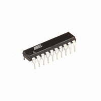
ATTINY26L-8PU Atmel, ATTINY26L-8PU Datasheet - Page 59

ATTINY26L-8PU
Manufacturer Part Number
ATTINY26L-8PU
Description
IC MCU AVR 2K 5V 8MHZ 20-DIP
Manufacturer
Atmel
Series
AVR® ATtinyr
Datasheets
1.ATTINY26-16MC.pdf
(18 pages)
2.ATTINY26-16MC.pdf
(182 pages)
3.ATTINY26L-8PU.pdf
(183 pages)
Specifications of ATTINY26L-8PU
Core Processor
AVR
Core Size
8-Bit
Speed
8MHz
Connectivity
USI
Peripherals
Brown-out Detect/Reset, POR, PWM, WDT
Number Of I /o
16
Program Memory Size
2KB (1K x 16)
Program Memory Type
FLASH
Eeprom Size
128 x 8
Ram Size
128 x 8
Voltage - Supply (vcc/vdd)
2.7 V ~ 5.5 V
Data Converters
A/D 11x10b
Oscillator Type
Internal
Operating Temperature
-40°C ~ 85°C
Package / Case
20-DIP (0.300", 7.62mm)
Processor Series
ATTINY2x
Core
AVR8
Data Bus Width
8 bit
Data Ram Size
128 B
Interface Type
2-Wire/ISP/SM-Bus/SPI/UART/USI
Maximum Clock Frequency
8 MHz
Number Of Programmable I/os
16
Number Of Timers
2
Operating Supply Voltage
2.7 V to 5.5 V
Maximum Operating Temperature
+ 85 C
Mounting Style
Through Hole
3rd Party Development Tools
EWAVR, EWAVR-BL
Development Tools By Supplier
ATAVRDRAGON, ATSTK500, ATSTK600, ATAVRISP2, ATAVRONEKIT
Minimum Operating Temperature
- 40 C
On-chip Adc
11-ch x 10-bit
Controller Family/series
AVR Tiny
No. Of I/o's
16
Eeprom Memory Size
128Byte
Ram Memory Size
128Byte
Cpu Speed
8MHz
Rohs Compliant
Yes
For Use With
ATSTK600 - DEV KIT FOR AVR/AVR32770-1007 - ISP 4PORT ATMEL AVR MCU SPI/JTAGATAVRISP2 - PROGRAMMER AVR IN SYSTEMATSTK505 - ADAPTER KIT FOR 14PIN AVR MCU
Lead Free Status / RoHS Status
Lead free / RoHS Compliant
Other names
ATTINY26L-8PJ
ATTINY26L-8PJ
ATTINY26L-8PJ
Available stocks
Company
Part Number
Manufacturer
Quantity
Price
Company:
Part Number:
ATTINY26L-8PU
Manufacturer:
Atmel
Quantity:
25 295
Part Number:
ATTINY26L-8PU
Manufacturer:
ATMEL/爱特梅尔
Quantity:
20 000
General Interrupt Flag
Register – GIFR
Timer/Counter Interrupt Mask
Register – TIMSK
1477F–AVR–12/04
interrupt is activated on rising or falling edge, on pin change, or low level of the INT0 pin.
Activity on the pin will cause an interrupt request even if INT0 is configured as an output.
The corresponding interrupt of External Interrupt Request 0 is executed from program
memory address $001. See also “External Interrupt” on page 62.
• Bit 5 – PCIE1: Pin Change Interrupt Enable1
When the PCIE1 bit is set (one) and the I-bit in the Status Register (SREG) is set (one),
the interrupt pin change is enabled on analog pins PB[7:4], PA[7:6] and PA[3]. Unless
the alternate function masks out the interrupt, any change on the pin mentioned before
will cause an interrupt. The corresponding interrupt of Pin Change Interrupt Request is
executed from program memory address $002. See also “Pin Change Interrupt” on
page 62.
• Bit 4– PCIE0: Pin Change Interrupt Enable0
When the PCIE0 bit is set (one) and the I-bit in the Status Register (SREG) is set (one),
the interrupt pin change is enabled on digital pins PB[3:0]. Unless the alternate function
masks out the interrupt, any change on the pin mentioned before will cause an interrupt.
The corresponding interrupt of Pin Change Interrupt Request is executed from program
memory address $002. See also “Pin Change Interrupt” on page 62.
• Bits 3..0 – Res: Reserved Bits
These bits are reserved bits in the ATtiny26(L) and always read as zero.
• Bit 7 – Res: Reserved Bit
This bit is a reserved bit in the ATtiny26(L) and always reads as zero.
• Bit 6 – INTF0: External Interrupt Flag0
When an event on the INT0 pin triggers an interrupt request, INTF0 becomes set (one).
If the I-bit in SREG and the INT0 bit in GIMSK are set (one), the MCU will jump to the
Interrupt Vector at address $001. The flag is cleared when the interrupt routine is exe-
cuted. Alternatively, the flag can be cleared by writing a logical one to it. The flag is
always cleared when INT0 is configured as level interrupt.
• Bit 5 – PCIF: Pin Change Interrupt Flag
When an event on pins PB[7:0], PA[7:6], or PA[3] triggers an interrupt request, PCIF
becomes set (one). PCIE1 enables interrupt from analog pins PB[7:4], PA[7:6], and
PA[3]. PCIE0 enables interrupt on digital pins PB[3:0]. Note that pin change interrupt
enable bits PCIE1 and PCIE0 also mask the flag if they are not set. For example, if
PCIE0 is cleared, a pin change on PB[3:0] does not set PCIF. If an alternate function is
enabled on a pin, PCIF is masked from that individual pin. If the I-bit in SREG and the
PCIE bit in GIMSK are set (one), the MCU will jump to the Interrupt Vector at address
$002. The flag is cleared when the interrupt routine is executed. Alternatively, the flag
can be cleared by writing a logical one to it. See also “Pin Change Interrupt” on page 62.
• Bits 4..0 – Res: Reserved Bits
These bits are reserved bits in the ATtiny26(L) and always read as zero.
Bit
$3A ($5A)
Read/Write
Initial Value
Bit
$39 ($59)
7
–
R
7
–
0
OCIE1A
INTF0
R/W
6
0
6
OCIE1B
PCIF
R/W
5
0
5
R
4
–
0
4
–
3
–
R
0
3
–
R
2
–
0
TOIE1
2
ATtiny26(L)
R
1
–
0
TOIE0
1
R
0
–
0
0
–
GIFR
TIMSK
59


