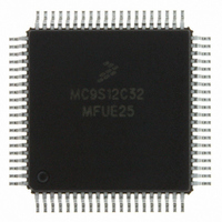
MC9S12C32MFUE25 Freescale Semiconductor, MC9S12C32MFUE25 Datasheet - Page 247

MC9S12C32MFUE25
Manufacturer Part Number
MC9S12C32MFUE25
Description
IC MCU 32K FLASH 25MHZ 80-QFP
Manufacturer
Freescale Semiconductor
Series
HCS12r
Datasheets
1.MC9S12GC16MFUE.pdf
(690 pages)
2.MC9S12C96CFUER.pdf
(26 pages)
3.MC9S12C32CFAE25.pdf
(2 pages)
Specifications of MC9S12C32MFUE25
Core Processor
HCS12
Core Size
16-Bit
Speed
25MHz
Connectivity
CAN, EBI/EMI, SCI, SPI
Peripherals
POR, PWM, WDT
Number Of I /o
60
Program Memory Size
32KB (32K x 8)
Program Memory Type
FLASH
Ram Size
2K x 8
Voltage - Supply (vcc/vdd)
2.35 V ~ 5.5 V
Data Converters
A/D 8x10b
Oscillator Type
Internal
Operating Temperature
-40°C ~ 125°C
Package / Case
80-QFP
Processor Series
S12C
Core
HCS12
Data Bus Width
16 bit
Data Ram Size
2 KB
Interface Type
CAN/SCI/SPI
Maximum Clock Frequency
25 MHz
Number Of Programmable I/os
60
Number Of Timers
8
Operating Supply Voltage
3.3 V to 5.5 V
Maximum Operating Temperature
+ 125 C
Mounting Style
SMD/SMT
3rd Party Development Tools
EWHCS12
Development Tools By Supplier
M68EVB912C32EE
Minimum Operating Temperature
- 40 C
On-chip Adc
8-ch x 10-bit
For Use With
CML12C32SLK - KIT STUDENT LEARNING 16BIT HCS12
Lead Free Status / RoHS Status
Lead free / RoHS Compliant
Eeprom Size
-
Lead Free Status / Rohs Status
Lead free / RoHS Compliant
Available stocks
Company
Part Number
Manufacturer
Quantity
Price
Company:
Part Number:
MC9S12C32MFUE25
Manufacturer:
Freescale Semiconductor
Quantity:
10 000
Part Number:
MC9S12C32MFUE25
Manufacturer:
FREESCALE
Quantity:
20 000
Company:
Part Number:
MC9S12C32MFUE25R
Manufacturer:
Freescale Semiconductor
Quantity:
10 000
- Current page: 247 of 690
- Download datasheet (4Mb)
8.4.2.2
The channel pins can be multiplexed between analog and digital data. As analog inputs, they are
multiplexed and sampled to supply signals to the A/D converter. Alternatively they can be configured as
digital I/O signals with the port I/O data being held in PORTAD.
The analog/digital multiplex operation is performed in the pads. The pad is always connected to the analog
inputs of the ATD10B8C. The pad signal is buffered to the digital port registers. This buffer can be turned
on or off with the ATDDIEN register. This is important so that the buffer does not draw excess current
when analog potentials are presented at its input.
8.4.2.3
The ATD10B8C can be configured for lower MCU power consumption in three different ways:
8.5
8.5.1
The following describes a typical setup procedure for starting A/D conversions. It is highly recommended
to follow this procedure to avoid common mistakes.
Each step of the procedure will have a general remark and a typical example
8.5.1.1
Power up the ATD and concurrently define other settings in ATDCTL2
Example: Write to ATDCTL2: ADPU=1 -> powers up the ATD, ASCIE=1 enable interrupt on finish of a
conversion sequence.
8.5.1.2
Wait for the ATD Recovery Time
Example: Use the CPU in a branch loop to wait for a defined number of bus clocks.
Freescale Semiconductor
1. Stop Mode: This halts A/D conversion. Exit from Stop mode will resume A/D conversion, But due
2. Wait Mode with AWAI = 1: This halts A/D conversion. Exit from Wait mode will resume A/D
3. Writing ADPU = 0 (Note that all ATD registers remain accessible.): This aborts any A/D
to the recovery time the result of this conversion should be ignored.
conversion, but due to the recovery time the result of this conversion should be ignored.
conversion in progress.
Initialization/Application Information
Setting up and starting an A/D conversion
General-Purpose Digital Port Operation
Low-Power Modes
Step 1
Step 2
The reset value for the ADPU bit is zero. Therefore, when this module is
reset, it is reset into the power down state.
t
REC
MC9S12C-Family / MC9S12GC-Family
before you proceed with Step 3.
Rev 01.24
NOTE
Chapter 8 Analog-to-Digital Converter (ATD10B8C) Block Description
247
Related parts for MC9S12C32MFUE25
Image
Part Number
Description
Manufacturer
Datasheet
Request
R
Part Number:
Description:
Manufacturer:
Freescale Semiconductor, Inc
Datasheet:
Part Number:
Description:
Manufacturer:
Freescale Semiconductor, Inc
Datasheet:
Part Number:
Description:
Manufacturer:
Freescale Semiconductor, Inc
Datasheet:
Part Number:
Description:
Manufacturer:
Freescale Semiconductor, Inc
Datasheet:
Part Number:
Description:
Manufacturer:
Freescale Semiconductor, Inc
Datasheet:
Part Number:
Description:
Manufacturer:
Freescale Semiconductor, Inc
Datasheet:
Part Number:
Description:
Manufacturer:
Freescale Semiconductor, Inc
Datasheet:
Part Number:
Description:
Manufacturer:
Freescale Semiconductor, Inc
Datasheet:
Part Number:
Description:
Manufacturer:
Freescale Semiconductor, Inc
Datasheet:
Part Number:
Description:
Manufacturer:
Freescale Semiconductor, Inc
Datasheet:
Part Number:
Description:
Manufacturer:
Freescale Semiconductor, Inc
Datasheet:
Part Number:
Description:
Manufacturer:
Freescale Semiconductor, Inc
Datasheet:
Part Number:
Description:
Manufacturer:
Freescale Semiconductor, Inc
Datasheet:
Part Number:
Description:
Manufacturer:
Freescale Semiconductor, Inc
Datasheet:
Part Number:
Description:
Manufacturer:
Freescale Semiconductor, Inc
Datasheet:


