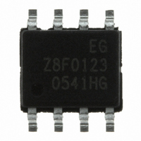
Z8F0123SB005EG Zilog, Z8F0123SB005EG Datasheet - Page 36

Z8F0123SB005EG
Manufacturer Part Number
Z8F0123SB005EG
Description
IC ENCORE MCU FLASH 1K 8SOIC
Manufacturer
Zilog
Series
Encore!® XP®r
Datasheet
1.Z8F0223SB005SG.pdf
(247 pages)
Specifications of Z8F0123SB005EG
Core Processor
Z8
Core Size
8-Bit
Speed
5MHz
Connectivity
IrDA, UART/USART
Peripherals
Brown-out Detect/Reset, LED, POR, PWM, WDT
Number Of I /o
6
Program Memory Size
1KB (1K x 8)
Program Memory Type
FLASH
Ram Size
256 x 8
Voltage - Supply (vcc/vdd)
2.7 V ~ 3.6 V
Data Converters
A/D 4x10b
Oscillator Type
Internal
Operating Temperature
-40°C ~ 105°C
Package / Case
8-SOIC (3.9mm Width)
Lead Free Status / RoHS Status
Lead free / RoHS Compliant
Eeprom Size
-
Other names
269-3757
- Current page: 36 of 247
- Download datasheet (4Mb)
Stop Mode Recovery
PS024314-0308
External Reset Indicator
On-Chip Debugger Initiated Reset
clock and reset signals, the required reset duration can be as short as three clock periods
and as long as four. A reset pulse three clock cycles in duration might trigger a reset; a
pulse four cycles in duration always triggers a reset.
While the RESET input pin is asserted Low, the Z8 Encore! XP F0823 Series devices
remain in the Reset state. If the RESET pin is held Low beyond the System Reset time-
out, the device exits the Reset state on the system clock rising edge following RESET pin
deassertion. Following a System Reset initiated by the external RESET pin, the EXT sta-
tus bit in the WDT Control (WDTCTL) register is set to 1.
During System Reset or when enabled by the GPIO logic (see
on page 44), the RESET pin functions as an open-drain (active Low) reset mode indicator
in addition to the input functionality. This reset output feature allows an Z8 Encore! XP
F0823 Series device to reset other components to which it is connected, even if that reset
is caused by internal sources such as POR, VBO, or WDT events.
After an internal reset event occurs, the internal circuitry begins driving the RESET pin
Low. The RESET pin is held Low by the internal circuitry until the appropriate delay
listed in
A POR is initiated using the On-Chip Debugger by setting the RST bit in the OCD Control
register. The OCD block is not reset but the rest of the chip goes through a normal system
reset. The RST bit automatically clears during the System Reset. Following the System
Reset, the POR bit in the Reset Status (RSTSTAT) register is set.
The device enters into STOP mode when eZ8 CPU executes a
details on STOP mode, see
the CPU is held in reset for 66 IPO cycles if the crystal oscillator is disabled or 5000
cycles if it is enabled. The SMR delay also included the time required to start up the IPO.
Stop Mode Recovery does not affect on-chip registers other than the Watchdog Timer
Control register (WDTCTL) and the Oscillator Control register (OSCCTL). After any
Stop Mode Recovery, the IPO is enabled and selected as the system clock. If another
system clock source is required or IPO disabling is required, the Stop Mode Recovery
code must reconfigure the oscillator control block such that the correct system clock
source is enabled and selected.
The eZ8 CPU fetches the Reset vector at Program Memory addresses
and loads that value into the Program Counter. Program execution begins at the Reset
Table 9
has elapsed.
Low-Power Modes
on page 31. During Stop Mode Recovery,
Z8 Encore! XP
Reset and Stop Mode Recovery
Port A–C Control Registers
STOP
Product Specification
instruction. For more
0002H
®
F0823 Series
and
0003H
26
Related parts for Z8F0123SB005EG
Image
Part Number
Description
Manufacturer
Datasheet
Request
R

Part Number:
Description:
Communication Controllers, ZILOG INTELLIGENT PERIPHERAL CONTROLLER (ZIP)
Manufacturer:
Zilog, Inc.
Datasheet:

Part Number:
Description:
KIT DEV FOR Z8 ENCORE 16K TO 64K
Manufacturer:
Zilog
Datasheet:

Part Number:
Description:
KIT DEV Z8 ENCORE XP 28-PIN
Manufacturer:
Zilog
Datasheet:

Part Number:
Description:
DEV KIT FOR Z8 ENCORE 8K/4K
Manufacturer:
Zilog
Datasheet:

Part Number:
Description:
KIT DEV Z8 ENCORE XP 28-PIN
Manufacturer:
Zilog
Datasheet:

Part Number:
Description:
DEV KIT FOR Z8 ENCORE 4K TO 8K
Manufacturer:
Zilog
Datasheet:

Part Number:
Description:
CMOS Z8 microcontroller. ROM 16 Kbytes, RAM 256 bytes, speed 16 MHz, 32 lines I/O, 3.0V to 5.5V
Manufacturer:
Zilog, Inc.
Datasheet:

Part Number:
Description:
Low-cost microcontroller. 512 bytes ROM, 61 bytes RAM, 8 MHz
Manufacturer:
Zilog, Inc.
Datasheet:

Part Number:
Description:
Z8 4K OTP Microcontroller
Manufacturer:
Zilog, Inc.
Datasheet:

Part Number:
Description:
CMOS SUPER8 ROMLESS MCU
Manufacturer:
Zilog, Inc.
Datasheet:

Part Number:
Description:
SL1866 CMOSZ8 OTP Microcontroller
Manufacturer:
Zilog, Inc.
Datasheet:

Part Number:
Description:
SL1866 CMOSZ8 OTP Microcontroller
Manufacturer:
Zilog, Inc.
Datasheet:

Part Number:
Description:
OTP (KB) = 1, RAM = 125, Speed = 12, I/O = 14, 8-bit Timers = 2, Comm Interfaces Other Features = Por, LV Protect, Voltage = 4.5-5.5V
Manufacturer:
Zilog, Inc.
Datasheet:

Part Number:
Description:
Manufacturer:
Zilog, Inc.
Datasheet:


