Z8F0123SB005EG Zilog, Z8F0123SB005EG Datasheet - Page 132
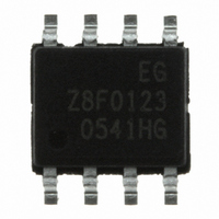
Z8F0123SB005EG
Manufacturer Part Number
Z8F0123SB005EG
Description
IC ENCORE MCU FLASH 1K 8SOIC
Manufacturer
Zilog
Series
Encore!® XP®r
Datasheet
1.Z8F0223SB005SG.pdf
(247 pages)
Specifications of Z8F0123SB005EG
Core Processor
Z8
Core Size
8-Bit
Speed
5MHz
Connectivity
IrDA, UART/USART
Peripherals
Brown-out Detect/Reset, LED, POR, PWM, WDT
Number Of I /o
6
Program Memory Size
1KB (1K x 8)
Program Memory Type
FLASH
Ram Size
256 x 8
Voltage - Supply (vcc/vdd)
2.7 V ~ 3.6 V
Data Converters
A/D 4x10b
Oscillator Type
Internal
Operating Temperature
-40°C ~ 105°C
Package / Case
8-SOIC (3.9mm Width)
Lead Free Status / RoHS Status
Lead free / RoHS Compliant
Eeprom Size
-
Other names
269-3757


Table 72. ADC Control Register 0 (ADCCTL0)
ADC Control Register Definitions
BITS
FIELD
RESET
R/W
ADDR
PS024314-0308
Note:
Caution:
ADC Control Register 0
CEN
R/W
ADC comp
7
0
Software Compensation Procedure
The value read from the ADC high and low byte registers are uncompensated. The user
mode software must apply gain and offset correction to this uncompensated value for
maximum accuracy. The following formula yields the compensated value:
where GAINCAL is the gain calibration byte, OFFCAL is the offset calibration byte and
ADC
two’s complement format, as are the compensated and uncompensated ADC values.
The offset compensation is performed first, followed by the gain compensation. One bit of
resolution is lost because of rounding on both the offset and gain computations. As a result
the ADC registers read back 13 bits: 1 sign bit, two calibration bits lost to rounding and
10 data bits. Also note that in the second term, the multiplication must be performed
before the division by 2
The following sections define the ADC control registers.
The ADC Control register selects the analog input channel and initiates the
analog-to-digital conversion.
CEN—Conversion Enable
0 = Conversion is complete. Writing a 0 produces no effect. The ADC automatically clears
this bit to 0 when a conversion is complete.
1 = Begin conversion. Writing a 1 to this bit starts a conversion. If a conversion is already
in progress, the conversion restarts. This bit remains 1 until the conversion is complete.
Although the ADC can be used without the gain and offset compensation, it does exhibit
non-unity gain. Designing the ADC with sub-unity gain reduces noise across the ADC
range but requires the ADC results to be scaled by a factor of 8/7.
uncomp
REFSELL
R/W
=
6
0
is the uncompensated value read from the ADC. The OFFCAL value is in
(
ADC uncomp OFFCAL
REFEXT
R/W
16
5
0
. Otherwise, the second term evaluates to zero incorrectly.
–
CONT
R/W
4
0
F70H
)
+
(
(
ADC uncomp OFFCAL
R/W
3
0
Z8 Encore! XP
R/W
–
2
0
ANAIN[3:0]
Product Specification
Analog-to-Digital Converter
R/W
) ∗ GAINCAL
1
0
®
F0823 Series
R/W
) 2 16
0
0
⁄
122
Related parts for Z8F0123SB005EG
Image
Part Number
Description
Manufacturer
Datasheet
Request
R

Part Number:
Description:
Communication Controllers, ZILOG INTELLIGENT PERIPHERAL CONTROLLER (ZIP)
Manufacturer:
Zilog, Inc.
Datasheet:

Part Number:
Description:
KIT DEV FOR Z8 ENCORE 16K TO 64K
Manufacturer:
Zilog
Datasheet:

Part Number:
Description:
KIT DEV Z8 ENCORE XP 28-PIN
Manufacturer:
Zilog
Datasheet:

Part Number:
Description:
DEV KIT FOR Z8 ENCORE 8K/4K
Manufacturer:
Zilog
Datasheet:

Part Number:
Description:
KIT DEV Z8 ENCORE XP 28-PIN
Manufacturer:
Zilog
Datasheet:

Part Number:
Description:
DEV KIT FOR Z8 ENCORE 4K TO 8K
Manufacturer:
Zilog
Datasheet:
Part Number:
Description:
CMOS Z8 microcontroller. ROM 16 Kbytes, RAM 256 bytes, speed 16 MHz, 32 lines I/O, 3.0V to 5.5V
Manufacturer:
Zilog, Inc.
Datasheet:
Part Number:
Description:
Low-cost microcontroller. 512 bytes ROM, 61 bytes RAM, 8 MHz
Manufacturer:
Zilog, Inc.
Datasheet:
Part Number:
Description:
Z8 4K OTP Microcontroller
Manufacturer:
Zilog, Inc.
Datasheet:
Part Number:
Description:
CMOS SUPER8 ROMLESS MCU
Manufacturer:
Zilog, Inc.
Datasheet:
Part Number:
Description:
SL1866 CMOSZ8 OTP Microcontroller
Manufacturer:
Zilog, Inc.
Datasheet:
Part Number:
Description:
SL1866 CMOSZ8 OTP Microcontroller
Manufacturer:
Zilog, Inc.
Datasheet:
Part Number:
Description:
OTP (KB) = 1, RAM = 125, Speed = 12, I/O = 14, 8-bit Timers = 2, Comm Interfaces Other Features = Por, LV Protect, Voltage = 4.5-5.5V
Manufacturer:
Zilog, Inc.
Datasheet:
Part Number:
Description:
Manufacturer:
Zilog, Inc.
Datasheet: