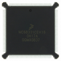
MC68331CEH16 Freescale Semiconductor, MC68331CEH16 Datasheet - Page 36

MC68331CEH16
Manufacturer Part Number
MC68331CEH16
Description
IC MCU 32BIT 16MHZ 132-PQFP
Manufacturer
Freescale Semiconductor
Series
M683xxr
Specifications of MC68331CEH16
Core Processor
CPU32
Core Size
32-Bit
Speed
16MHz
Connectivity
EBI/EMI, SCI, SPI, UART/USART
Peripherals
POR, PWM, WDT
Number Of I /o
18
Program Memory Type
ROMless
Voltage - Supply (vcc/vdd)
4.5 V ~ 5.5 V
Oscillator Type
Internal
Operating Temperature
-40°C ~ 85°C
Package / Case
132-QFP
Package
132PQFP
Device Core
ColdFire
Family Name
68K/M683xx
Maximum Speed
16 MHz
Ram Size
80 Byte
Data Bus Width
32 Bit
Number Of Programmable I/os
18
Interface Type
QSPI/SCI/UART
Number Of Timers
1
Processor Series
M683xx
Core
CPU32
Eeprom Memory
0 Bytes
Input Output
18
Interface
EBI/EMI, SCI, SPI, UART/USART
Ios
18
Memory Type
ROMless
Number Of Bits
32
Package Type
132-pin QFP
Programmable Memory
0 Bytes
Voltage, Range
4.5-5.5 V
Controller Family/series
68K
No. Of I/o's
18
Cpu Speed
16MHz
No. Of Timers
1
Embedded Interface Type
QSPI, SCI, UART
No. Of Pwm Channels
2
Digital Ic Case Style
PQFP
Rohs Compliant
Yes
Data Ram Size
80 B
Maximum Clock Frequency
16 MHz
Maximum Operating Temperature
+ 85 C
Mounting Style
SMD/SMT
Minimum Operating Temperature
- 40 C
Lead Free Status / RoHS Status
Lead free / RoHS Compliant
Eeprom Size
-
Ram Size
-
Program Memory Size
-
Data Converters
-
Lead Free Status / Rohs Status
Lead free / RoHS Compliant
Available stocks
Company
Part Number
Manufacturer
Quantity
Price
Company:
Part Number:
MC68331CEH16
Manufacturer:
Freescale Semiconductor
Quantity:
10 000
Part Number:
MC68331CEH16
Manufacturer:
FREESCALE
Quantity:
20 000
PORTF0, PORTF1 — Port F Data Register
DDRF — Port F Data Direction Register
PFPAR — Port F Pin Assignment Register
36
RESET:
RESET:
RESET:
15
15
15
The write to the port F data register is stored in the internal data latch, and if any port F pin is configured
as an output, the value stored for that bit is driven onto the pin. A read of the port F data register returns
the value at the pin only if the pin is configured as a discrete input. Otherwise, the value read is the value
stored in the register.
The port F data register is a single register that can be accessed in two locations. When accessed at
$YFFA19, the register is referred to as PORTF0; when accessed at $YFFA1B, the register is referred
to as PORTF1. The register can be read or written at any time. It is unaffected by reset.
The bits in this register control the direction of the pin drivers when the pins are configured for I/O. Any
bit in this register set to one configures the corresponding pin as an output. Any bit in this register
cleared to zero configures the corresponding pin as an input.
The bits in this register control the function of each port F pin. Any bit cleared to zero defines the corre-
sponding pin to be an I/O pin. Any bit set to one defines the corresponding pin to be an interrupt request
signal or MODCLK. The MODCLK signal has no function after reset.
Data bus pin 9 controls the state of this register following reset. If DATA9 is set to one during reset, the
register is set to $FF, which defines all port F pins as interrupt request inputs. If DATA9 is cleared to
zero during reset, this register is set to $00, defining all port F pins as I/O pins.
PFPAR Field
NOT USED
NOT USED
NOT USED
PFPA7
PFPA6
PFPA5
PFPA4
PFPA3
PFPA2
PFPA1
PFPA0
Freescale Semiconductor, Inc.
For More Information On This Product,
Table 17 Port F Pin Assignments
Go to: www.freescale.com
Port F Signal
8
8
8
PF7
PF6
PF5
PF4
PF3
PF2
PF1
PF0
DATA9 DATA9 DATA9 DATA9 DATA9 DATA9 DATA9 DATA9
PFPA7 PFPA6 PFPA5 PFPA4 PFPA3 PFPA2 PFPA1 PFPA0
DDF7
PF7
7
U
7
0
7
DDF6
PF6
U
6
6
0
6
DDF5
PF5
U
5
5
0
5
Alternate Signal
MODCLK
DDF4
IRQ7
IRQ6
IRQ5
IRQ4
IRQ3
IRQ2
IRQ1
PF4
U
4
4
0
4
DDF3
PF3
U
3
3
0
3
$YFFA19, $YFFA1B
DDF2
PF2
U
2
2
0
2
MC68331TS/D
DDF1
PF1
$YFFA1D
U
1
1
0
$YFFA1F
1
DDF0
PF0
0
U
0
0
0


