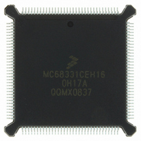
MC68331CEH16 Freescale Semiconductor, MC68331CEH16 Datasheet - Page 31

MC68331CEH16
Manufacturer Part Number
MC68331CEH16
Description
IC MCU 32BIT 16MHZ 132-PQFP
Manufacturer
Freescale Semiconductor
Series
M683xxr
Specifications of MC68331CEH16
Core Processor
CPU32
Core Size
32-Bit
Speed
16MHz
Connectivity
EBI/EMI, SCI, SPI, UART/USART
Peripherals
POR, PWM, WDT
Number Of I /o
18
Program Memory Type
ROMless
Voltage - Supply (vcc/vdd)
4.5 V ~ 5.5 V
Oscillator Type
Internal
Operating Temperature
-40°C ~ 85°C
Package / Case
132-QFP
Package
132PQFP
Device Core
ColdFire
Family Name
68K/M683xx
Maximum Speed
16 MHz
Ram Size
80 Byte
Data Bus Width
32 Bit
Number Of Programmable I/os
18
Interface Type
QSPI/SCI/UART
Number Of Timers
1
Processor Series
M683xx
Core
CPU32
Eeprom Memory
0 Bytes
Input Output
18
Interface
EBI/EMI, SCI, SPI, UART/USART
Ios
18
Memory Type
ROMless
Number Of Bits
32
Package Type
132-pin QFP
Programmable Memory
0 Bytes
Voltage, Range
4.5-5.5 V
Controller Family/series
68K
No. Of I/o's
18
Cpu Speed
16MHz
No. Of Timers
1
Embedded Interface Type
QSPI, SCI, UART
No. Of Pwm Channels
2
Digital Ic Case Style
PQFP
Rohs Compliant
Yes
Data Ram Size
80 B
Maximum Clock Frequency
16 MHz
Maximum Operating Temperature
+ 85 C
Mounting Style
SMD/SMT
Minimum Operating Temperature
- 40 C
Lead Free Status / RoHS Status
Lead free / RoHS Compliant
Eeprom Size
-
Ram Size
-
Program Memory Size
-
Data Converters
-
Lead Free Status / Rohs Status
Lead free / RoHS Compliant
Available stocks
Company
Part Number
Manufacturer
Quantity
Price
Company:
Part Number:
MC68331CEH16
Manufacturer:
Freescale Semiconductor
Quantity:
10 000
Part Number:
MC68331CEH16
Manufacturer:
FREESCALE
Quantity:
20 000
3.5.3 Base Address Registers
CSBARBT — Chip-Select Base Address Register Boot ROM
CSBAR[10:0] —Chip-Select Base Address Registers
BLKSZ —Block Size Field
MC68331TS/D
RESET:
RESET:
ADDR
ADDR
15
23
15
23
0
0
data register (PORTC), with the following exceptions:
At reset, either the alternate function (01) or chip-select function (11) can be encoded. DATA pins are
driven to logic level one by a weak internal pull-up during reset. Encoding is for chip-select function un-
less a data line is held low during reset. Note that bus loading can overcome the weak pull-up and hold
pins low during reset. The following table shows the hierarchical selection method that determines the
reset functions of pins controlled by CSPAR1.
A pin programmed as a discrete output drives an external signal to the value specified in the port C pin
When a pin is programmed for discrete output or alternate function, internal chip-select logic still func-
tions and can be used to generate DSACK or AVEC internally on an address match.
Port size is determined when a pin is assigned as a chip select. When a pin is assigned to an 8-bit port,
the chip select is asserted at all addresses within the block range. If a pin is assigned to a 16-bit port,
the upper/lower byte field of the option register selects the byte with which the chip select is associated.
A base address is the starting address for the block enabled by a given chip select. Block size deter-
mines the extent of the block above the base address. Each chip select has an associated base register
so that an efficient address map can be constructed for each application. If a chip-select base address
register is programmed with the same address as a microcontroller module or memory array, an access
to that address goes to the module or array and the chip-select signal is not asserted.
This field determines the size of the block that must be enabled by the chip select. The following table
shows bit encoding for the base address registers block size field.
DATA7
A. No discrete output function is available on pins BR, BG, or BGACK.
B. ADDR23 provides E-clock output rather than a discrete output signal.
1
1
1
1
1
0
ADDR
ADDR
14
22
14
22
0
0
DATA6
ADDR
ADDR
13
21
13
21
Data Bus Pins at Reset
0
0
X
1
1
1
1
0
ADDR
ADDR
12
20
12
20
0
0
DATA5
Freescale Semiconductor, Inc.
X
X
1
1
1
0
ADDR
ADDR
11
19
11
19
0
For More Information On This Product,
0
Table 15 Reset Pin Function of CS[10:6]
DATA4
ADDR
ADDR
10
18
10
18
0
0
1
1
0
X
X
X
Go to: www.freescale.com
ADDR
ADDR
17
17
0
9
0
9
DATA3
1
0
X
X
X
X
ADDR
ADDR
16
16
0
8
0
8
ADDR23
ADDR23 ADDR22 ADDR21 ADDR20 ADDR19
ADDR
ADDR
CS10/
CS10
CS10
CS10
CS10
CS10
15
15
0
7
0
7
Chip-Select/Address Bus Pin Function
ADDR
ADDR
14
14
0
6
0
6
ADDR22
ADDR22 ADDR21 ADDR20 ADDR19
CS9/
CS9
CS9
CS9
CS9
ADDR
ADDR
13
13
0
5
0
5
ADDR21
ADDR21 ADDR20 ADDR19
ADDR
ADDR
CS8/
CS8
CS8
CS8
12
12
0
4
0
4
ADDR
ADDR
11
11
0
3
0
3
ADDR20
ADDR20 ADDR19
$YFFA4C–$YFFA74
CS7/
CS7
CS7
0
2
1
2
ADDR19
ADDR19
BLKSZ
BLKSZ
CS6/
CS6
0
$YFFA48
1
0
0
1
0
31


