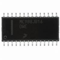
MC908JB16DWE Freescale Semiconductor, MC908JB16DWE Datasheet - Page 256

MC908JB16DWE
Manufacturer Part Number
MC908JB16DWE
Description
IC MCU 16K FLASH 6MHZ USB 28SOIC
Manufacturer
Freescale Semiconductor
Series
HC08r
Specifications of MC908JB16DWE
Core Processor
HC08
Core Size
8-Bit
Speed
6MHz
Connectivity
SCI, USB
Peripherals
LED, LVD, POR, PWM
Number Of I /o
21
Program Memory Size
16KB (16K x 8)
Program Memory Type
FLASH
Ram Size
384 x 8
Voltage - Supply (vcc/vdd)
4 V ~ 5.5 V
Oscillator Type
Internal
Operating Temperature
0°C ~ 70°C
Package / Case
28-SOIC (7.5mm Width)
Processor Series
HC08JB
Core
HC08
Data Bus Width
8 bit
Data Ram Size
384 B
Interface Type
I2C/SCI/SPI/USB
Maximum Clock Frequency
12 MHz
Number Of Programmable I/os
21
Number Of Timers
4
Operating Supply Voltage
5.5 V
Maximum Operating Temperature
+ 70 C
Mounting Style
SMD/SMT
Development Tools By Supplier
FSICEBASE, DEMO908GZ60E, M68EML08GZE, KITUSBSPIDGLEVME, KITUSBSPIEVME, KIT33810EKEVME
Minimum Operating Temperature
0 C
Controller Family/series
HC08
No. Of I/o's
21
Ram Memory Size
384Byte
Cpu Speed
8MHz
No. Of Timers
2
Embedded Interface Type
I2C, SCI, SPI
Rohs Compliant
Yes
Lead Free Status / RoHS Status
Lead free / RoHS Compliant
Eeprom Size
-
Data Converters
-
Lead Free Status / Rohs Status
Lead free / RoHS Compliant
Available stocks
Company
Part Number
Manufacturer
Quantity
Price
Company:
Part Number:
MC908JB16DWE
Manufacturer:
FREESCALE
Quantity:
1 831
Part Number:
MC908JB16DWE
Manufacturer:
FRE/MOT
Quantity:
20 000
- Current page: 256 of 332
- Download datasheet (4Mb)
Clock Generator Module (CGM)
13.9.1 Bandwidth Control Register
13.9.2 VCO Control Register (PVCR)
Technical Data
256
Address:
Address:
Reset:
Reset:
The bandwidth control register (PBWC) contains control/status bits for
both PLLs.
LOCKx — Lock Indicator Bit
PLLONx — PLL On Bit
The VCO control register configures the VCO for both PLLs.
VCO_[7:0] — VCO Control Bits for both PLLs
Read:
Write:
Read:
Write:
This read-only bit becomes set when the VCO clock is locked (running
at the programmed frequency).
This read/write bit activates each PLL and enables the VCO clock.
Set VCO_[7:0] = $80 for maximum performance.
1 = VCO frequency correct or locked
0 = VCO frequency incorrect or unlocked
1 = PLL on
0 = PLL off
Figure 13-6. PLL Bandwidth Control Register (PBCR)
VCO_7
$0051
$0052
Bit 7
Bit 7
R
0
Clock Generator Module (CGM)
Figure 13-7. VCO Control Register (PVCR)
= Unimplemented
LOCK1
VCO_6
6
0
6
0
VCO_5
R
5
5
1
PLLON1
VCO_4
4
0
4
1
VCO_3
R
R
3
3
0
MC68HC908JB16
= Reserved
LOCK2
VCO_2
Freescale Semiconductor
2
0
2
0
VCO_1
R
1
1
0
—
PLLON2
Rev. 1.1
VCO_0
Bit 0
Bit 0
0
0
Related parts for MC908JB16DWE
Image
Part Number
Description
Manufacturer
Datasheet
Request
R
Part Number:
Description:
Manufacturer:
Freescale Semiconductor, Inc
Datasheet:
Part Number:
Description:
Manufacturer:
Freescale Semiconductor, Inc
Datasheet:
Part Number:
Description:
Manufacturer:
Freescale Semiconductor, Inc
Datasheet:
Part Number:
Description:
Manufacturer:
Freescale Semiconductor, Inc
Datasheet:
Part Number:
Description:
Manufacturer:
Freescale Semiconductor, Inc
Datasheet:
Part Number:
Description:
Manufacturer:
Freescale Semiconductor, Inc
Datasheet:
Part Number:
Description:
Manufacturer:
Freescale Semiconductor, Inc
Datasheet:
Part Number:
Description:
Manufacturer:
Freescale Semiconductor, Inc
Datasheet:
Part Number:
Description:
Manufacturer:
Freescale Semiconductor, Inc
Datasheet:
Part Number:
Description:
Manufacturer:
Freescale Semiconductor, Inc
Datasheet:
Part Number:
Description:
Manufacturer:
Freescale Semiconductor, Inc
Datasheet:
Part Number:
Description:
Manufacturer:
Freescale Semiconductor, Inc
Datasheet:
Part Number:
Description:
Manufacturer:
Freescale Semiconductor, Inc
Datasheet:
Part Number:
Description:
Manufacturer:
Freescale Semiconductor, Inc
Datasheet:
Part Number:
Description:
Manufacturer:
Freescale Semiconductor, Inc
Datasheet:


