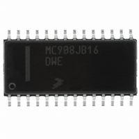
MC908JB16DWE Freescale Semiconductor, MC908JB16DWE Datasheet - Page 264

MC908JB16DWE
Manufacturer Part Number
MC908JB16DWE
Description
IC MCU 16K FLASH 6MHZ USB 28SOIC
Manufacturer
Freescale Semiconductor
Series
HC08r
Specifications of MC908JB16DWE
Core Processor
HC08
Core Size
8-Bit
Speed
6MHz
Connectivity
SCI, USB
Peripherals
LED, LVD, POR, PWM
Number Of I /o
21
Program Memory Size
16KB (16K x 8)
Program Memory Type
FLASH
Ram Size
384 x 8
Voltage - Supply (vcc/vdd)
4 V ~ 5.5 V
Oscillator Type
Internal
Operating Temperature
0°C ~ 70°C
Package / Case
28-SOIC (7.5mm Width)
Processor Series
HC08JB
Core
HC08
Data Bus Width
8 bit
Data Ram Size
384 B
Interface Type
I2C/SCI/SPI/USB
Maximum Clock Frequency
12 MHz
Number Of Programmable I/os
21
Number Of Timers
4
Operating Supply Voltage
5.5 V
Maximum Operating Temperature
+ 70 C
Mounting Style
SMD/SMT
Development Tools By Supplier
FSICEBASE, DEMO908GZ60E, M68EML08GZE, KITUSBSPIDGLEVME, KITUSBSPIEVME, KIT33810EKEVME
Minimum Operating Temperature
0 C
Controller Family/series
HC08
No. Of I/o's
21
Ram Memory Size
384Byte
Cpu Speed
8MHz
No. Of Timers
2
Embedded Interface Type
I2C, SCI, SPI
Rohs Compliant
Yes
Lead Free Status / RoHS Status
Lead free / RoHS Compliant
Eeprom Size
-
Data Converters
-
Lead Free Status / Rohs Status
Lead free / RoHS Compliant
Available stocks
Company
Part Number
Manufacturer
Quantity
Price
Company:
Part Number:
MC908JB16DWE
Manufacturer:
FREESCALE
Quantity:
1 831
Part Number:
MC908JB16DWE
Manufacturer:
FRE/MOT
Quantity:
20 000
- Current page: 264 of 332
- Download datasheet (4Mb)
Input/Output (I/O) Ports
Technical Data
264
* DDRA7 bit is reset by POR or LVI reset only.
Addr.
$0000
$0001
$0002
$0003
$0004
$0005
$0006
$0007
$0008
Data Direction Register C
Data Direction Register D
Data Direction Register A
Register Name
Port C Data Register
Port D Data Register
Port A Data Register
Port E Data Register
NOTE:
Reserved
Reserved
(DDRC)
(DDRD)
(DDRA)
(PTA)
(PTC)
(PTD)
(PTE)
Connect any unused I/O pins to an appropriate logic level, either V
V
operation, termination reduces excess current consumption and the
possibility of electrostatic damage.
Reset:
Reset:
Reset:
Reset:
Reset:
Reset:
Reset:
Reset:
Reset:
SS
Read:
Read:
Read:
Read:
Read:
Read:
Read:
Read:
Read:
Write:
Write:
Write:
Write:
Write:
Write:
Write:
Write:
Write:
Figure 14-1. I/O Port Register Summary
. Although the I/O ports do not require termination for proper
DDRA7
PTA7
Bit 7
0*
R
R
0
0
0
0
0
0
0
Input/Output (I/O) Ports
= Unimplemented
DDRA6
PTA6
R
R
6
0
0
0
0
0
0
0
0
DDRA5
DDRD5
PTA5
PTD5
R
R
5
0
0
0
0
0
0
Unaffected by reset
Unaffected by reset
Unaffected by reset
DDRA4
DDRD4
Unaffected by reset
PTA4
PTD4
PTE4
R
R
4
0
0
0
0
0
DDRA3
DDRD3
PTA3
PTD3
PTE3
R
R
R
3
0
0
0
0
0
MC68HC908JB16
= Reserved
DDRD2
DDRA2
PTA2
PTD2
PTE2
Freescale Semiconductor
R
R
0
0
0
0
0
2
DDRC1
DDRD1
DDRA1
PTA1
PTC1
PTD1
PTE1
R
R
1
0
0
0
—
DDRC0
DDRD0
Rev. 1.1
DDRA0
PTA0
PTC0
PTD0
PTE0
Bit 0
DD
R
R
0
0
0
or
Related parts for MC908JB16DWE
Image
Part Number
Description
Manufacturer
Datasheet
Request
R
Part Number:
Description:
Manufacturer:
Freescale Semiconductor, Inc
Datasheet:
Part Number:
Description:
Manufacturer:
Freescale Semiconductor, Inc
Datasheet:
Part Number:
Description:
Manufacturer:
Freescale Semiconductor, Inc
Datasheet:
Part Number:
Description:
Manufacturer:
Freescale Semiconductor, Inc
Datasheet:
Part Number:
Description:
Manufacturer:
Freescale Semiconductor, Inc
Datasheet:
Part Number:
Description:
Manufacturer:
Freescale Semiconductor, Inc
Datasheet:
Part Number:
Description:
Manufacturer:
Freescale Semiconductor, Inc
Datasheet:
Part Number:
Description:
Manufacturer:
Freescale Semiconductor, Inc
Datasheet:
Part Number:
Description:
Manufacturer:
Freescale Semiconductor, Inc
Datasheet:
Part Number:
Description:
Manufacturer:
Freescale Semiconductor, Inc
Datasheet:
Part Number:
Description:
Manufacturer:
Freescale Semiconductor, Inc
Datasheet:
Part Number:
Description:
Manufacturer:
Freescale Semiconductor, Inc
Datasheet:
Part Number:
Description:
Manufacturer:
Freescale Semiconductor, Inc
Datasheet:
Part Number:
Description:
Manufacturer:
Freescale Semiconductor, Inc
Datasheet:
Part Number:
Description:
Manufacturer:
Freescale Semiconductor, Inc
Datasheet:


