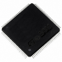
ST92F150CV1TB STMicroelectronics, ST92F150CV1TB Datasheet - Page 424

ST92F150CV1TB
Manufacturer Part Number
ST92F150CV1TB
Description
MCU 8BIT 128K FLASH 100TQFP
Manufacturer
STMicroelectronics
Series
ST9r
Datasheet
1.ST92F150CV1TB.pdf
(429 pages)
Specifications of ST92F150CV1TB
Core Processor
ST9
Core Size
8/16-Bit
Speed
24MHz
Connectivity
CAN, EBI/EMI, I²C, LIN, SCI, SPI
Peripherals
DMA, LVD, POR, PWM, WDT
Number Of I /o
77
Program Memory Size
128KB (128K x 8)
Program Memory Type
FLASH
Eeprom Size
1K x 8
Ram Size
4K x 8
Voltage - Supply (vcc/vdd)
4.5 V ~ 5.5 V
Data Converters
A/D 16x10b
Oscillator Type
Internal
Operating Temperature
-40°C ~ 105°C
Package / Case
100-TQFP, 100-VQFP
Processor Series
ST92F15x
Core
ST9
Data Bus Width
8 bit, 16 bit
Data Ram Size
6 KB
Interface Type
CAN, I2C, SCI, SPI
Maximum Clock Frequency
24 MHz
Number Of Programmable I/os
80
Number Of Timers
5 x 16 bit
Operating Supply Voltage
4.5 V to 5.5 V
Maximum Operating Temperature
+ 105 C
Mounting Style
SMD/SMT
Development Tools By Supplier
ST92F150-EPB
Minimum Operating Temperature
- 40 C
On-chip Adc
16 bit x 10 bit
Lead Free Status / RoHS Status
Lead free / RoHS Compliant
Other names
497-4883
Available stocks
Company
Part Number
Manufacturer
Quantity
Price
Company:
Part Number:
ST92F150CV1TB
Manufacturer:
STMicroelectronics
Quantity:
10 000
- Current page: 424 of 429
- Download datasheet (8Mb)
ST92F124/F150/F250 - KNOWN LIMITATIONS
KNOWN LIMITATIONS (Cont’d)
During reset, the risk of power consumption in the
input stage due to floating inputs is avoided by a
design feature.
However, if the application requires pull-ups
during reset (for instance, in order to send known
logic values to external devices), external pull-ups
must be provided. When the I/O port outputs a
zero, there will be some additional power con-
sumption as these external pull-ups are not
switched off.
These ports behave in the same way following an
external, watchdog or software reset.
13.8.2 High Drive I/Os when BSZ=1
Description
If the BSZ bit in the EMR1 register (bit 1 of R245,
page 21) is set so as to use high-drive output
buffers for P4[7:6] and P6[5:4], all I/O ports as well
as AS, DS and RW will also use high-drive output
buffers.
Impact On Application
P0[7:0], AS, DS and RW have the same V
rameter value as P6[5:4].
P0[7:0]-P2[3:2], AS, DS and RW have the same
V
P6[5:4].
These I/Os using high-drive output buffers will
generate more noise than those using the
standard low-noise output buffers.
13.8.3 ADC PARASITIC DIODE
Description
A parasitic diode is present between an ADC input
and AV
As described in the datasheet, the user has the
possibility to switch off AV
the ADC to save power consumption. However, if
AV
present on the Input Port, an increase in power
consumption can occur.
424/429
1
OL
DD
and I
is connected to ground and a voltage is
DD
IO
.
parameter values as the P4[7:6] and
DD
when he switches off
OH
pa-
The Input Port affected by this diode is the one
pointed to by the analog multiplexer of the ADC, if
the port is set up as AF analog input. When the
ADC is stopped, the multiplexer points to the first
input to be converted in a scan (i.e. the channel
pointed to by the SC[3:0] bits).
Workaround
In order to avoid this problem, the I/O connected to
the ADC has to be set up in any mode except AF
analog input (i.e. any combination of PxC2.. PxC0
except 111).
1. Deprogram analog input mode from the I/O port
2. Next, switch off the A/D Converter.
The current in AV
logic levels on the analog inputs, and whatever the
voltage level applied to AV
V
13.8.4
INJECTION CURRENT
Description
If a negative current is injected to an input pin (i.e.
input signal voltage below -0.3V), a part of this cur-
rent will be drawn from the adjacent I/Os. The fol-
lowing curve quantifies this current:
DD
which is pointed to by the SC[3:0] bits (start
conversion channel, b7..b4 of CLR1).
For example the I/O can be reprogrammed as
an open drain output, with the data at 1. The
high impedance of the output stage then
avoids a conflict with the external voltage
source. In order to avoid potential power con-
sumption in the input buffer of this I/O,
depending on the external voltage applied to
the pin, it is wise to set the 'start conversion
channel' to a channel which carries levels
below 800 mV or above (V
Another possibility is to modify the SC[3:0]
bits so that they point to an I/O Port which is
not used as an analog input.
).
ADC
ACCURACY
DD
will be zero, whatever the
DD
DD
VS.
(between 0 and
- 800 mV).
NEGATIVE
Related parts for ST92F150CV1TB
Image
Part Number
Description
Manufacturer
Datasheet
Request
R

Part Number:
Description:
BOARD PROGRAM FOR ST92F150 MCU
Manufacturer:
STMicroelectronics
Datasheet:

Part Number:
Description:
BOARD EVALUATION FOR ST9 SERIES
Manufacturer:
STMicroelectronics
Datasheet:

Part Number:
Description:
BOARD EMULATOR FOR ST9 SERIES
Manufacturer:
STMicroelectronics
Datasheet:

Part Number:
Description:
MCU, MPU & DSP Development Tools ST9 Dedication Board
Manufacturer:
STMicroelectronics
Datasheet:

Part Number:
Description:
STMicroelectronics [RIPPLE-CARRY BINARY COUNTER/DIVIDERS]
Manufacturer:
STMicroelectronics
Datasheet:

Part Number:
Description:
STMicroelectronics [LIQUID-CRYSTAL DISPLAY DRIVERS]
Manufacturer:
STMicroelectronics
Datasheet:

Part Number:
Description:
BOARD EVAL FOR MEMS SENSORS
Manufacturer:
STMicroelectronics
Datasheet:

Part Number:
Description:
NPN TRANSISTOR POWER MODULE
Manufacturer:
STMicroelectronics
Datasheet:

Part Number:
Description:
TURBOSWITCH ULTRA-FAST HIGH VOLTAGE DIODE
Manufacturer:
STMicroelectronics
Datasheet:

Part Number:
Description:
Manufacturer:
STMicroelectronics
Datasheet:

Part Number:
Description:
DIODE / SCR MODULE
Manufacturer:
STMicroelectronics
Datasheet:

Part Number:
Description:
DIODE / SCR MODULE
Manufacturer:
STMicroelectronics
Datasheet:


