ST92F150CV1TB STMicroelectronics, ST92F150CV1TB Datasheet - Page 124
ST92F150CV1TB
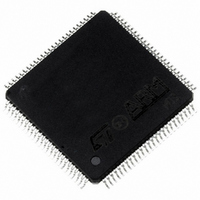
Manufacturer Part Number
ST92F150CV1TB
Description
MCU 8BIT 128K FLASH 100TQFP
Manufacturer
STMicroelectronics
Series
ST9r
Datasheet
1.ST92F150CV1TB.pdf
(429 pages)
Specifications of ST92F150CV1TB
Core Processor
ST9
Core Size
8/16-Bit
Speed
24MHz
Connectivity
CAN, EBI/EMI, I²C, LIN, SCI, SPI
Peripherals
DMA, LVD, POR, PWM, WDT
Number Of I /o
77
Program Memory Size
128KB (128K x 8)
Program Memory Type
FLASH
Eeprom Size
1K x 8
Ram Size
4K x 8
Voltage - Supply (vcc/vdd)
4.5 V ~ 5.5 V
Data Converters
A/D 16x10b
Oscillator Type
Internal
Operating Temperature
-40°C ~ 105°C
Package / Case
100-TQFP, 100-VQFP
Processor Series
ST92F15x
Core
ST9
Data Bus Width
8 bit, 16 bit
Data Ram Size
6 KB
Interface Type
CAN, I2C, SCI, SPI
Maximum Clock Frequency
24 MHz
Number Of Programmable I/os
80
Number Of Timers
5 x 16 bit
Operating Supply Voltage
4.5 V to 5.5 V
Maximum Operating Temperature
+ 105 C
Mounting Style
SMD/SMT
Development Tools By Supplier
ST92F150-EPB
Minimum Operating Temperature
- 40 C
On-chip Adc
16 bit x 10 bit
Lead Free Status / RoHS Status
Lead free / RoHS Compliant
Other names
497-4883
Available stocks
Company
Part Number
Manufacturer
Quantity
Price
Company:

Part Number:
ST92F150CV1TB
Manufacturer:
STMicroelectronics
Quantity:
10 000


ST92F124/F150/F250 - ON-CHIP DIRECT MEMORY ACCESS (DMA)
DMA TRANSACTIONS (Cont’d)
6.4 DMA CYCLE TIME
The interrupt and DMA arbitration protocol func-
tions completely asynchronously from instruction
flow.
Requests are sampled every 5 CPUCLK cycles.
DMA transactions are executed if their priority al-
lows it.
A DMA transfer with the Register file requires 8
CPUCLK cycles.
A DMA transfer with memory requires 16 CPUCLK
cycles, plus any required wait states.
6.5 SWAP MODE
An extra feature which may be found on the DMA
channels of some peripherals (e.g. the MultiFunc-
tion Timer) is the Swap mode. This feature allows
n
124/429
9
transfer from two DMA tables alternatively. All the
DMA descriptors in the Register File are thus dou-
bled. Two DMA transaction counters and two DMA
address pointers allow the definition of two fully in-
dependent tables (they only have to belong to the
same space, Register File or Memory). The DMA
transaction is programmed to start on one of the
two tables (say table 0) and, at the end of the
block, the DMA controller automatically swaps to
the other table (table 1) by pointing to the other
DMA descriptors. In this case, the DMA mask (DM
bit) control bit is not cleared, but the End Of Block
interrupt request is generated to allow the optional
updating of the first data table (table 0).
Until the swap mode is disabled, the DMA control-
ler will continue to swap between DMA Table 0
and DMA Table 1.
Related parts for ST92F150CV1TB
Image
Part Number
Description
Manufacturer
Datasheet
Request
R

Part Number:
Description:
BOARD PROGRAM FOR ST92F150 MCU
Manufacturer:
STMicroelectronics
Datasheet:
Part Number:
Description:
BOARD EVALUATION FOR ST9 SERIES
Manufacturer:
STMicroelectronics
Datasheet:
Part Number:
Description:
BOARD EMULATOR FOR ST9 SERIES
Manufacturer:
STMicroelectronics
Datasheet:
Part Number:
Description:
MCU, MPU & DSP Development Tools ST9 Dedication Board
Manufacturer:
STMicroelectronics
Datasheet:
Part Number:
Description:
STMicroelectronics [RIPPLE-CARRY BINARY COUNTER/DIVIDERS]
Manufacturer:
STMicroelectronics
Datasheet:
Part Number:
Description:
STMicroelectronics [LIQUID-CRYSTAL DISPLAY DRIVERS]
Manufacturer:
STMicroelectronics
Datasheet:

Part Number:
Description:
BOARD EVAL FOR MEMS SENSORS
Manufacturer:
STMicroelectronics
Datasheet:
Part Number:
Description:
NPN TRANSISTOR POWER MODULE
Manufacturer:
STMicroelectronics
Datasheet:
Part Number:
Description:
TURBOSWITCH ULTRA-FAST HIGH VOLTAGE DIODE
Manufacturer:
STMicroelectronics
Datasheet:
Part Number:
Description:
Manufacturer:
STMicroelectronics
Datasheet:
Part Number:
Description:
DIODE / SCR MODULE
Manufacturer:
STMicroelectronics
Datasheet:
Part Number:
Description:
DIODE / SCR MODULE
Manufacturer:
STMicroelectronics
Datasheet: