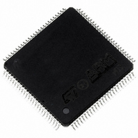
ST92F150CV1TB STMicroelectronics, ST92F150CV1TB Datasheet - Page 148

ST92F150CV1TB
Manufacturer Part Number
ST92F150CV1TB
Description
MCU 8BIT 128K FLASH 100TQFP
Manufacturer
STMicroelectronics
Series
ST9r
Datasheet
1.ST92F150CV1TB.pdf
(429 pages)
Specifications of ST92F150CV1TB
Core Processor
ST9
Core Size
8/16-Bit
Speed
24MHz
Connectivity
CAN, EBI/EMI, I²C, LIN, SCI, SPI
Peripherals
DMA, LVD, POR, PWM, WDT
Number Of I /o
77
Program Memory Size
128KB (128K x 8)
Program Memory Type
FLASH
Eeprom Size
1K x 8
Ram Size
4K x 8
Voltage - Supply (vcc/vdd)
4.5 V ~ 5.5 V
Data Converters
A/D 16x10b
Oscillator Type
Internal
Operating Temperature
-40°C ~ 105°C
Package / Case
100-TQFP, 100-VQFP
Processor Series
ST92F15x
Core
ST9
Data Bus Width
8 bit, 16 bit
Data Ram Size
6 KB
Interface Type
CAN, I2C, SCI, SPI
Maximum Clock Frequency
24 MHz
Number Of Programmable I/os
80
Number Of Timers
5 x 16 bit
Operating Supply Voltage
4.5 V to 5.5 V
Maximum Operating Temperature
+ 105 C
Mounting Style
SMD/SMT
Development Tools By Supplier
ST92F150-EPB
Minimum Operating Temperature
- 40 C
On-chip Adc
16 bit x 10 bit
Lead Free Status / RoHS Status
Lead free / RoHS Compliant
Other names
497-4883
Available stocks
Company
Part Number
Manufacturer
Quantity
Price
Company:
Part Number:
ST92F150CV1TB
Manufacturer:
STMicroelectronics
Quantity:
10 000
- Current page: 148 of 429
- Download datasheet (8Mb)
ST92F124/F150/F250 - EXTERNAL MEMORY INTERFACE (EXTMI)
8.3 REGISTER DESCRIPTION
EXTERNAL MEMORY REGISTER 1 (EMR1)
R245 - Read/Write
Register Page: 21
Reset value: 1000 0000 (80h)
Bit 7 = Reserved.
Bit 6 = MC: Mode Control.
0: AS, DS and RW pins have the standard ST9 for-
1: AS pin becomes ALE, Address Load Enable.
Bit 5 = DS2EN: Data Strobe 2 enable.
0: The DS pin is active for any external memory
1: If the lower memory block is addressed, the
148/429
9
X
7
mat.
This signal indicates to the external address
latch that a valid address is put on AD[7:0].
When ALE is high, the multiplexed address/data
bus AD[7:0] carries the LSBs of the memory ad-
dress, which must be latched on the falling edge
of this signal.
DS becomes OEN, Output ENable: When this
signal is low, the external memory should put
the data on the multiplexed address/data bus
AD[7:0]. The data is sampled by the microcon-
troller on the rising edge of the OEN signal.
RW pin becomes WEN, Write ENable: when this
signal is low, the multiplexed address/data bus
AD[7:0] carries the data to be written in the ex-
ternal memory. The external memory should
sample the data on the rising edge of the WEN
signal.
access (lower and upper memory block).
The DS2 pin remains high.
DS2 pin outputs the standard DS signal, while
the DS pin stays high during the whole memory
cycle.
MC
DS2EN
ASAF
0
ETO
BSZ
0
X
Refer to
Bit 4 = ASAF: Address Strobe as Alternate Func-
tion.
Depending on the device, AS can be either a ded-
icated pin or a port Alternate Function. This bit is
used only in the second case.
0: AS Alternate function disabled.
1: AS Alternate Function enabled.
Bit 3 = Reserved, must be kept cleared.
Bit 2 = ETO: External toggle.
0: The external memory interface pins (AS, DS,
1: When the internal memory protection is dis-
Bit 1 = BSZ: Bus size.
0: All outputs use the standard low-noise output
1: P4[7:6], P6[5:4] use high-drive output buffers
Bit 0 = Reserved.
Caution: External memory must be correctly ad-
dressed before and after a write operation on the
EMR1 register. For example, if code is fetched
from external memory using the standard ST9 ex-
ternal memory interface configuration (MC=0),
setting the MC bit will cause the device to behave
unpredictably.
If the upper memory block is addressed, DS2 is
forced to “1” during the whole memory cycle.
DS2, RW, Port0, Port1, Port9) toggle only if an
access to external memory is performed.
abled, the above pins (except DS which never
toggles during internal memory accesses) tog-
gle during both internal and external memory
accesses.
buffers.
Figure 77
Related parts for ST92F150CV1TB
Image
Part Number
Description
Manufacturer
Datasheet
Request
R

Part Number:
Description:
BOARD PROGRAM FOR ST92F150 MCU
Manufacturer:
STMicroelectronics
Datasheet:

Part Number:
Description:
BOARD EVALUATION FOR ST9 SERIES
Manufacturer:
STMicroelectronics
Datasheet:

Part Number:
Description:
BOARD EMULATOR FOR ST9 SERIES
Manufacturer:
STMicroelectronics
Datasheet:

Part Number:
Description:
MCU, MPU & DSP Development Tools ST9 Dedication Board
Manufacturer:
STMicroelectronics
Datasheet:

Part Number:
Description:
STMicroelectronics [RIPPLE-CARRY BINARY COUNTER/DIVIDERS]
Manufacturer:
STMicroelectronics
Datasheet:

Part Number:
Description:
STMicroelectronics [LIQUID-CRYSTAL DISPLAY DRIVERS]
Manufacturer:
STMicroelectronics
Datasheet:

Part Number:
Description:
BOARD EVAL FOR MEMS SENSORS
Manufacturer:
STMicroelectronics
Datasheet:

Part Number:
Description:
NPN TRANSISTOR POWER MODULE
Manufacturer:
STMicroelectronics
Datasheet:

Part Number:
Description:
TURBOSWITCH ULTRA-FAST HIGH VOLTAGE DIODE
Manufacturer:
STMicroelectronics
Datasheet:

Part Number:
Description:
Manufacturer:
STMicroelectronics
Datasheet:

Part Number:
Description:
DIODE / SCR MODULE
Manufacturer:
STMicroelectronics
Datasheet:

Part Number:
Description:
DIODE / SCR MODULE
Manufacturer:
STMicroelectronics
Datasheet:


