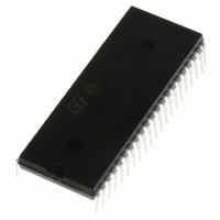
ST72F324BJ6B6 STMicroelectronics, ST72F324BJ6B6 Datasheet - Page 59

ST72F324BJ6B6
Manufacturer Part Number
ST72F324BJ6B6
Description
MCU 8BIT 32KB FLASH/ROM 42-SDIP
Manufacturer
STMicroelectronics
Series
ST7r
Datasheet
1.ST72F324BJ6B6.pdf
(193 pages)
Specifications of ST72F324BJ6B6
Core Processor
ST7
Core Size
8-Bit
Speed
8MHz
Connectivity
SCI, SPI
Peripherals
LVD, POR, PWM, WDT
Number Of I /o
32
Program Memory Size
32KB (32K x 8)
Program Memory Type
FLASH
Ram Size
1K x 8
Voltage - Supply (vcc/vdd)
3.8 V ~ 5.5 V
Data Converters
A/D 12x10b
Oscillator Type
Internal
Operating Temperature
-40°C ~ 85°C
Package / Case
42-SDIP (0.600", 15.24mm)
Controller Family/series
ST7
No. Of I/o's
32
Ram Memory Size
1KB
Cpu Speed
8MHz
No. Of Timers
2
Embedded Interface Type
SCI, SPI
No. Of Pwm Channels
3
Processor Series
ST72F3x
Core
ST7
Data Bus Width
8 bit
Data Ram Size
1 KB
Interface Type
SCI, SPI
Maximum Clock Frequency
8 MHz
Number Of Programmable I/os
32
Number Of Timers
3
Maximum Operating Temperature
+ 85 C
Mounting Style
Through Hole
Development Tools By Supplier
ST7232X-EVAL, ST7MDT20-DVP3, ST7MDT20J-EMU3, STX-RLINK
Minimum Operating Temperature
- 40 C
On-chip Adc
10 bit, 12 Channel
For Use With
497-6421 - BOARD EVAL DGTL BATT CHGR DESIGN497-5046 - KIT TOOL FOR ST7/UPSD/STR7 MCU
Lead Free Status / RoHS Status
Lead free / RoHS Compliant
Eeprom Size
-
Lead Free Status / Rohs Status
Details
Other names
497-5589-5
- Current page: 59 of 193
- Download datasheet (3Mb)
ST72324Bxx
9.2.2
9.2.3
Note:
External interrupt function
When an I/O is configured as ‘Input with Interrupt’, an event on this I/O can generate an
external interrupt request to the CPU.
Each pin can independently generate an interrupt request. The interrupt sensitivity is
independently programmable using the sensitivity bits in the EICR register.
Each external interrupt vector is linked to a dedicated group of I/O port pins (see pinout
description and interrupt section). If several input pins are selected simultaneously as
interrupt sources, these are first detected according to the sensitivity bits in the EICR
register and then logically ORed.
The external interrupts are hardware interrupts, which means that the request latch (not
accessible directly by the application) is automatically cleared when the corresponding
interrupt vector is fetched. To clear an unwanted pending interrupt by software, the
sensitivity bits in the EICR register must be modified.
Output modes
The output configuration is selected by setting the corresponding DDR register bit. In this
case, writing the DR register applies this digital value to the I/O pin through the latch. Then
reading the DR register returns the previously stored value.
Two different output modes can be selected by software through the OR register: Output
push-pull and open-drain.
Table 27.
Alternate functions
When an on-chip peripheral is configured to use a pin, the alternate function is automatically
selected. This alternate function takes priority over the standard I/O programming.
When the signal is coming from an on-chip peripheral, the I/O pin is automatically
configured in output mode (push-pull or open drain according to the peripheral).
When the signal is going to an on-chip peripheral, the I/O pin must be configured in input
mode. In this case, the pin state is also digitally readable by addressing the DR register.
Input pull-up configuration can cause unexpected value at the input of the alternate
peripheral input. When an on-chip peripheral use a pin as input and output, this pin has to
be configured in input floating mode.
DR
0
1
DR register value and output pin status
Push-pull
V
V
DD
SS
Open-drain
Floating
V
SS
I/O ports
59/193
Related parts for ST72F324BJ6B6
Image
Part Number
Description
Manufacturer
Datasheet
Request
R

Part Number:
Description:
STMicroelectronics [RIPPLE-CARRY BINARY COUNTER/DIVIDERS]
Manufacturer:
STMicroelectronics
Datasheet:

Part Number:
Description:
STMicroelectronics [LIQUID-CRYSTAL DISPLAY DRIVERS]
Manufacturer:
STMicroelectronics
Datasheet:

Part Number:
Description:
BOARD EVAL FOR MEMS SENSORS
Manufacturer:
STMicroelectronics
Datasheet:

Part Number:
Description:
NPN TRANSISTOR POWER MODULE
Manufacturer:
STMicroelectronics
Datasheet:

Part Number:
Description:
TURBOSWITCH ULTRA-FAST HIGH VOLTAGE DIODE
Manufacturer:
STMicroelectronics
Datasheet:

Part Number:
Description:
Manufacturer:
STMicroelectronics
Datasheet:

Part Number:
Description:
DIODE / SCR MODULE
Manufacturer:
STMicroelectronics
Datasheet:

Part Number:
Description:
DIODE / SCR MODULE
Manufacturer:
STMicroelectronics
Datasheet:

Part Number:
Description:
Search -----> STE16N100
Manufacturer:
STMicroelectronics
Datasheet:

Part Number:
Description:
Search ---> STE53NA50
Manufacturer:
STMicroelectronics
Datasheet:

Part Number:
Description:
NPN Transistor Power Module
Manufacturer:
STMicroelectronics
Datasheet:


