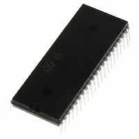
ST72F324BJ6B6 STMicroelectronics, ST72F324BJ6B6 Datasheet - Page 113

ST72F324BJ6B6
Manufacturer Part Number
ST72F324BJ6B6
Description
MCU 8BIT 32KB FLASH/ROM 42-SDIP
Manufacturer
STMicroelectronics
Series
ST7r
Datasheet
1.ST72F324BJ6B6.pdf
(193 pages)
Specifications of ST72F324BJ6B6
Core Processor
ST7
Core Size
8-Bit
Speed
8MHz
Connectivity
SCI, SPI
Peripherals
LVD, POR, PWM, WDT
Number Of I /o
32
Program Memory Size
32KB (32K x 8)
Program Memory Type
FLASH
Ram Size
1K x 8
Voltage - Supply (vcc/vdd)
3.8 V ~ 5.5 V
Data Converters
A/D 12x10b
Oscillator Type
Internal
Operating Temperature
-40°C ~ 85°C
Package / Case
42-SDIP (0.600", 15.24mm)
Controller Family/series
ST7
No. Of I/o's
32
Ram Memory Size
1KB
Cpu Speed
8MHz
No. Of Timers
2
Embedded Interface Type
SCI, SPI
No. Of Pwm Channels
3
Processor Series
ST72F3x
Core
ST7
Data Bus Width
8 bit
Data Ram Size
1 KB
Interface Type
SCI, SPI
Maximum Clock Frequency
8 MHz
Number Of Programmable I/os
32
Number Of Timers
3
Maximum Operating Temperature
+ 85 C
Mounting Style
Through Hole
Development Tools By Supplier
ST7232X-EVAL, ST7MDT20-DVP3, ST7MDT20J-EMU3, STX-RLINK
Minimum Operating Temperature
- 40 C
On-chip Adc
10 bit, 12 Channel
For Use With
497-6421 - BOARD EVAL DGTL BATT CHGR DESIGN497-5046 - KIT TOOL FOR ST7/UPSD/STR7 MCU
Lead Free Status / RoHS Status
Lead free / RoHS Compliant
Eeprom Size
-
Lead Free Status / Rohs Status
Details
Other names
497-5589-5
- Current page: 113 of 193
- Download datasheet (3Mb)
ST72324Bxx
Note:
Break characters
Setting the SBK bit loads the shift register with a break character. The break frame length
depends on the M bit (see
As long as the SBK bit is set, the SCI send break frames to the TDO pin. After clearing this
bit by software the SCI insert a logic 1 bit at the end of the last break frame to guarantee the
recognition of the start bit of the next frame.
Idle characters
Setting the TE bit drives the SCI to send an idle frame before the first data frame.
Clearing and then setting the TE bit during a transmission sends an idle frame after the
current word.
Resetting and setting the TE bit causes the data in the TDR register to be lost. Therefore,
the best time to toggle the TE bit is when the TDRE bit is set, that is, before writing the next
byte in the SCIDR.
Receiver
The SCI can receive data words of either 8 or 9 bits. When the M bit is set, word length is 9
bits and the MSB is stored in the R8 bit in the SCICR1 register.
Character reception
During a SCI reception, data shifts in least significant bit first through the RDI pin. In this
mode, the SCIDR register consists or a buffer (RDR) between the internal bus and the
received shift register (see
Procedure
1.
2.
3.
When a character is received:
●
●
●
Clearing the RDRF bit is performed by the following software sequence done by:
1. An access to the SCISR register
2. A read to the SCIDR register.
The RDRF bit must be cleared before the end of the reception of the next character to avoid
an overrun error.
Break character
When a break character is received, the SCI handles it as a framing error.
Idle character
When a idle frame is detected, there is the same procedure as a data received character
plus an interrupt if the ILIE bit is set and the I bit is cleared in the CCR register.
Select the M bit to define the word length.
Select the desired baud rate using the SCIBRR and the SCIERPR registers.
Set the RE bit, this enables the receiver which begins searching for a start bit.
The RDRF bit is set. It indicates that the content of the shift register is transferred to the
RDR.
An interrupt is generated if the RIE bit is set and the I bit is cleared in the CCR register.
The error flags can be set if a frame error, noise or an overrun error has been detected
during reception.
Figure
Figure
58).
57).
On-chip peripherals
113/193
Related parts for ST72F324BJ6B6
Image
Part Number
Description
Manufacturer
Datasheet
Request
R

Part Number:
Description:
STMicroelectronics [RIPPLE-CARRY BINARY COUNTER/DIVIDERS]
Manufacturer:
STMicroelectronics
Datasheet:

Part Number:
Description:
STMicroelectronics [LIQUID-CRYSTAL DISPLAY DRIVERS]
Manufacturer:
STMicroelectronics
Datasheet:

Part Number:
Description:
BOARD EVAL FOR MEMS SENSORS
Manufacturer:
STMicroelectronics
Datasheet:

Part Number:
Description:
NPN TRANSISTOR POWER MODULE
Manufacturer:
STMicroelectronics
Datasheet:

Part Number:
Description:
TURBOSWITCH ULTRA-FAST HIGH VOLTAGE DIODE
Manufacturer:
STMicroelectronics
Datasheet:

Part Number:
Description:
Manufacturer:
STMicroelectronics
Datasheet:

Part Number:
Description:
DIODE / SCR MODULE
Manufacturer:
STMicroelectronics
Datasheet:

Part Number:
Description:
DIODE / SCR MODULE
Manufacturer:
STMicroelectronics
Datasheet:

Part Number:
Description:
Search -----> STE16N100
Manufacturer:
STMicroelectronics
Datasheet:

Part Number:
Description:
Search ---> STE53NA50
Manufacturer:
STMicroelectronics
Datasheet:

Part Number:
Description:
NPN Transistor Power Module
Manufacturer:
STMicroelectronics
Datasheet:


