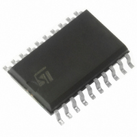
ST7FLITE19F1M6 STMicroelectronics, ST7FLITE19F1M6 Datasheet - Page 82

ST7FLITE19F1M6
Manufacturer Part Number
ST7FLITE19F1M6
Description
IC MCU 8BIT 4K 20-SOIC
Manufacturer
STMicroelectronics
Series
ST7r
Datasheet
1.ST7FLITE15F1M6.pdf
(131 pages)
Specifications of ST7FLITE19F1M6
Core Processor
ST7
Core Size
8-Bit
Speed
8MHz
Connectivity
SPI
Peripherals
LVD, POR, PWM, WDT
Number Of I /o
15
Program Memory Size
4KB (4K x 8)
Program Memory Type
FLASH
Eeprom Size
128 x 8
Ram Size
256 x 8
Voltage - Supply (vcc/vdd)
2.4 V ~ 5.5 V
Data Converters
A/D 7x10b
Oscillator Type
Internal
Operating Temperature
-40°C ~ 85°C
Package / Case
20-SOIC (7.5mm Width)
Processor Series
ST7FLITE1x
Core
ST7
Data Bus Width
8 bit
Data Ram Size
256 B
Interface Type
SPI
Maximum Clock Frequency
8 MHz
Number Of Programmable I/os
15
Number Of Timers
1 x 12 bit / 2 x 8 bit
Operating Supply Voltage
2.4 V to 5.5 V
Maximum Operating Temperature
+ 85 C
Mounting Style
SMD/SMT
Development Tools By Supplier
ST7FLIT2-COS/COM, ST7FLITE-SK/RAIS, ST7MDT10-DVP3, ST7MDT10-EMU3, STX-RLINK
Minimum Operating Temperature
- 40 C
On-chip Adc
7 bit x 10 bit
For Use With
497-5858 - EVAL BOARD PLAYBACK ST7FLITE497-5049 - KIT STARTER RAISONANCE ST7FLITE497-5046 - KIT TOOL FOR ST7/UPSD/STR7 MCU
Lead Free Status / RoHS Status
Contains lead / RoHS non-compliant
Other names
497-2133-5
Available stocks
Company
Part Number
Manufacturer
Quantity
Price
ST7LITE1
10-BIT A/D CONVERTER (ADC) (Cont’d)
11.5.3.2 Input Voltage Amplifier
The input voltage can be amplified by a factor of 8
by enabling the AMPSEL bit in the ADCDRL regis-
ter.
When the amplifier is enabled, the input range is
0V to V
For example, if V
vert voltages in the range 0V to 430mV with an
ideal resolution of 0.6mV (equivalent to 13-bit res-
olution with reference to a V
For more details, refer to the Electrical character-
istics section.
Note: The amplifier is switched on by the ADON
bit in the ADCCSR register, so no additional start-
up time is required when the amplifier is selected
by the AMPSEL bit.
11.5.3.3 Digital A/D Conversion Result
The conversion is monotonic, meaning that the re-
sult never decreases if the analog input does not
and never increases if the analog input does not.
If the input voltage (V
(high-level voltage reference) then the conversion
result is FFh in the ADCDRH register and 03h in
the ADCDRL register (without overflow indication).
If the input voltage (V
level voltage reference) then the conversion result
in the ADCDRH and ADCDRL registers is 00 00h.
The A/D converter is linear and the digital result of
the conversion is stored in the ADCDRH and AD-
CDRL registers. The accuracy of the conversion is
described in the Electrical Characteristics Section.
R
for an analog input signal. If the impedance is too
high, this will result in a loss of accuracy due to
leakage and sampling not being completed in the
alloted time.
11.5.3.4 A/D Conversion
The analog input ports must be configured as in-
put, no pull-up, no interrupt. Refer to the «I/O
ports» chapter. Using these pins as analog inputs
does not affect the ability of the port to be read as
a logic input.
In the ADCCSR register:
82/131
1
AIN
– Select the CS[2:0] bits to assign the analog
channel to convert.
is the maximum recommended impedance
DD
/8.
DD
= 5V, then the ADC can con-
AIN
AIN
) is lower than V
) is greater than V
SS
to V
DD
range).
SSA
(low-
DDA
ADC Conversion mode
In the ADCCSR register:
Set the ADON bit to enable the A/D converter and
When a conversion is complete:
A read to the ADCDRH resets the EOC bit.
To read the 10 bits, perform the following steps:
1. Poll EOC bit
2. Read ADCDRL
3. Read ADCDRH. This clears EOC automati-
To read only 8 bits, perform the following steps:
1. Poll EOC bit
2. Read ADCDRH. This clears EOC automati-
11.5.4 Low Power Modes
Note: The A/D converter may be disabled by re-
setting the ADON bit. This feature allows reduced
power consumption when no conversion is need-
ed and between single shot conversions.
11.5.5 Interrupts
None.
Mode
WAIT
HALT
to start the conversion. From this time on, the
ADC performs a continuous conversion of the
selected channel.
– The EOC bit is set by hardware.
– The result is in the ADCDR registers.
cally.
cally.
Description
No effect on A/D Converter
A/D Converter disabled.
After wakeup from Halt mode, the A/D
Converter requires a stabilization time
t
before accurate conversions can be
performed.
STAB
(see Electrical Characteristics)


