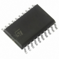
ST7FLITE19F1M6 STMicroelectronics, ST7FLITE19F1M6 Datasheet - Page 18

ST7FLITE19F1M6
Manufacturer Part Number
ST7FLITE19F1M6
Description
IC MCU 8BIT 4K 20-SOIC
Manufacturer
STMicroelectronics
Series
ST7r
Datasheet
1.ST7FLITE15F1M6.pdf
(131 pages)
Specifications of ST7FLITE19F1M6
Core Processor
ST7
Core Size
8-Bit
Speed
8MHz
Connectivity
SPI
Peripherals
LVD, POR, PWM, WDT
Number Of I /o
15
Program Memory Size
4KB (4K x 8)
Program Memory Type
FLASH
Eeprom Size
128 x 8
Ram Size
256 x 8
Voltage - Supply (vcc/vdd)
2.4 V ~ 5.5 V
Data Converters
A/D 7x10b
Oscillator Type
Internal
Operating Temperature
-40°C ~ 85°C
Package / Case
20-SOIC (7.5mm Width)
Processor Series
ST7FLITE1x
Core
ST7
Data Bus Width
8 bit
Data Ram Size
256 B
Interface Type
SPI
Maximum Clock Frequency
8 MHz
Number Of Programmable I/os
15
Number Of Timers
1 x 12 bit / 2 x 8 bit
Operating Supply Voltage
2.4 V to 5.5 V
Maximum Operating Temperature
+ 85 C
Mounting Style
SMD/SMT
Development Tools By Supplier
ST7FLIT2-COS/COM, ST7FLITE-SK/RAIS, ST7MDT10-DVP3, ST7MDT10-EMU3, STX-RLINK
Minimum Operating Temperature
- 40 C
On-chip Adc
7 bit x 10 bit
For Use With
497-5858 - EVAL BOARD PLAYBACK ST7FLITE497-5049 - KIT STARTER RAISONANCE ST7FLITE497-5046 - KIT TOOL FOR ST7/UPSD/STR7 MCU
Lead Free Status / RoHS Status
Contains lead / RoHS non-compliant
Other names
497-2133-5
Available stocks
Company
Part Number
Manufacturer
Quantity
Price
ST7LITE1
DATA EEPROM (Cont’d)
5.4 POWER SAVING MODES
Wait mode
The DATA EEPROM can enter WAIT mode on ex-
ecution of the WFI instruction of the microcontrol-
ler or when the microcontroller enters Active-HALT
mode.The DATA EEPROM will immediately enter
this mode if there is no programming in progress,
otherwise the DATA EEPROM will finish the cycle
and then enter WAIT mode.
Active-Halt mode
Refer to Wait mode.
Halt mode
The DATA EEPROM immediately enters HALT
mode if the microcontroller executes the HALT in-
struction. Therefore the EEPROM will stop the
function in progress, and data may be corrupted.
Figure 8. Data EEPROM Programming Cycle
18/131
1
INTERNAL
PROGRAMMING
VOLTAGE
DATA LATCHES
WRITE OF
ERASE CYCLE
READ OPERATION NOT POSSIBLE
t
PROG
5.5 ACCESS ERROR HANDLING
If a read access occurs while E2LAT=1, then the
data bus will not be driven.
If a write access occurs while E2LAT=0, then the
data on the bus will not be latched.
If a programming cycle is interrupted (by software/
RESET action), the memory data will not be guar-
anteed.
5.6 Data EEPROM Read-out Protection
The read-out protection is enabled through an op-
tion bit (see
When this option is selected, the programs and
data stored in the EEPROM memory are protected
against read-out (including a re-write protection).
In Flash devices, when this protection is removed
by reprogramming the Option Byte, the entire Pro-
gram memory and EEPROM is first automatically
erased.
Note: Both Program Memory and data EEPROM
are protected using the same option bit.
WRITE CYCLE
section 15.1 on page
READ OPERATION POSSIBLE
121).
PGM
LAT


