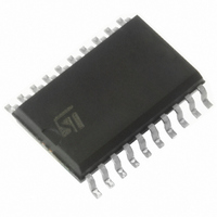
ST7FLITE19F1M6 STMicroelectronics, ST7FLITE19F1M6 Datasheet - Page 114

ST7FLITE19F1M6
Manufacturer Part Number
ST7FLITE19F1M6
Description
IC MCU 8BIT 4K 20-SOIC
Manufacturer
STMicroelectronics
Series
ST7r
Datasheet
1.ST7FLITE15F1M6.pdf
(131 pages)
Specifications of ST7FLITE19F1M6
Core Processor
ST7
Core Size
8-Bit
Speed
8MHz
Connectivity
SPI
Peripherals
LVD, POR, PWM, WDT
Number Of I /o
15
Program Memory Size
4KB (4K x 8)
Program Memory Type
FLASH
Eeprom Size
128 x 8
Ram Size
256 x 8
Voltage - Supply (vcc/vdd)
2.4 V ~ 5.5 V
Data Converters
A/D 7x10b
Oscillator Type
Internal
Operating Temperature
-40°C ~ 85°C
Package / Case
20-SOIC (7.5mm Width)
Processor Series
ST7FLITE1x
Core
ST7
Data Bus Width
8 bit
Data Ram Size
256 B
Interface Type
SPI
Maximum Clock Frequency
8 MHz
Number Of Programmable I/os
15
Number Of Timers
1 x 12 bit / 2 x 8 bit
Operating Supply Voltage
2.4 V to 5.5 V
Maximum Operating Temperature
+ 85 C
Mounting Style
SMD/SMT
Development Tools By Supplier
ST7FLIT2-COS/COM, ST7FLITE-SK/RAIS, ST7MDT10-DVP3, ST7MDT10-EMU3, STX-RLINK
Minimum Operating Temperature
- 40 C
On-chip Adc
7 bit x 10 bit
For Use With
497-5858 - EVAL BOARD PLAYBACK ST7FLITE497-5049 - KIT STARTER RAISONANCE ST7FLITE497-5046 - KIT TOOL FOR ST7/UPSD/STR7 MCU
Lead Free Status / RoHS Status
Contains lead / RoHS non-compliant
Other names
497-2133-5
Available stocks
Company
Part Number
Manufacturer
Quantity
Price
ST7LITE1
13.11 10-BIT ADC CHARACTERISTICS
Subject to general operating condition for V
Figure 87. Typical Application with ADC
Notes:
1. Unless otherwise specified, typical data are based on T
lines and are not tested.
2. When V
3. Any added external serial resistor will downgrade the ADC accuracy (especially for resistance greater than 10kΩ). Data
based on characterization results, not tested in production.
4. The stabilization time of the AD converter is masked by the fi
rst t
114/131
Symbol
C
t
R
f
V
t
I
STAB
ADC
ADC
ADC
LOAD
ADC
AIN
AIN
. The first conversion after the enable is then always valid.
DDA
ADC clock frequency
Conversion voltage range
External input resistor
Internal sample and hold capacitor
Stabilization time after ADC enable
Conversion time (Sample+Hold)
- Sample capacitor loading time
- Hold conversion time
Analog Part
Digital Part
V
and V
AIN
SSA
Parameter
pins are not available on the pinout, the ADC refers to V
R
AIN
C
AIN
2)
AINx
f
DD
CPU
, f
=8MHz, f
OSC
Conditions
A
=25°C and V
, and T
V
DD
ADC
V
0.6V
V
0.6V
T
T
=4MHz
A
unless otherwise specified.
DD
-V
SS
=5V. They are given only as design guide-
I
±1µA
L
V
Min
SSA
DD
and V
Typ
SS
10-Bit A/D
Conversion
0
3.5
10
6
4
.
4)
1)
V
10
Max
0.2
DDA
4
1
3)
ST72XXX
C
6pF
1/f
ADC
Unit
MHz
mA
kΩ
pF
µs
V
ADC


