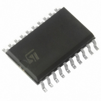
ST7FLITE19F1M6 STMicroelectronics, ST7FLITE19F1M6 Datasheet - Page 111

ST7FLITE19F1M6
Manufacturer Part Number
ST7FLITE19F1M6
Description
IC MCU 8BIT 4K 20-SOIC
Manufacturer
STMicroelectronics
Series
ST7r
Datasheet
1.ST7FLITE15F1M6.pdf
(131 pages)
Specifications of ST7FLITE19F1M6
Core Processor
ST7
Core Size
8-Bit
Speed
8MHz
Connectivity
SPI
Peripherals
LVD, POR, PWM, WDT
Number Of I /o
15
Program Memory Size
4KB (4K x 8)
Program Memory Type
FLASH
Eeprom Size
128 x 8
Ram Size
256 x 8
Voltage - Supply (vcc/vdd)
2.4 V ~ 5.5 V
Data Converters
A/D 7x10b
Oscillator Type
Internal
Operating Temperature
-40°C ~ 85°C
Package / Case
20-SOIC (7.5mm Width)
Processor Series
ST7FLITE1x
Core
ST7
Data Bus Width
8 bit
Data Ram Size
256 B
Interface Type
SPI
Maximum Clock Frequency
8 MHz
Number Of Programmable I/os
15
Number Of Timers
1 x 12 bit / 2 x 8 bit
Operating Supply Voltage
2.4 V to 5.5 V
Maximum Operating Temperature
+ 85 C
Mounting Style
SMD/SMT
Development Tools By Supplier
ST7FLIT2-COS/COM, ST7FLITE-SK/RAIS, ST7MDT10-DVP3, ST7MDT10-EMU3, STX-RLINK
Minimum Operating Temperature
- 40 C
On-chip Adc
7 bit x 10 bit
For Use With
497-5858 - EVAL BOARD PLAYBACK ST7FLITE497-5049 - KIT STARTER RAISONANCE ST7FLITE497-5046 - KIT TOOL FOR ST7/UPSD/STR7 MCU
Lead Free Status / RoHS Status
Contains lead / RoHS non-compliant
Other names
497-2133-5
Available stocks
Company
Part Number
Manufacturer
Quantity
Price
CONTROL PIN CHARACTERISTICS (Cont’d)
Figure 82. RESET pin protection when LVD is enabled.
Figure 83. RESET pin protection when LVD is disabled.
1. The reset network protects the device against parasitic resets.
2. The output of the external reset circuit must have an open-drain output to drive the ST7 reset pad. Otherwise the device
can be damaged when the ST7 generates an internal reset (LVD or watchdog).
3. Whatever the reset source is (internal or external), the user must ensure that the level on the RESET pin can go below
the V
4. Because the reset circuit is designed to allow the internal RESET to be output in the RESET pin, the user must ensure
that the current sunk on the RESET pin (by an external pull-up for example) is less than the absolute maximum value
specified for I
5. When the LVD is enabled, it is mandatory not to to connect a pull-up resistor and a capacitor to V
Required
EXTERNAL
CIRCUIT
RESET
IL
USER
max. level specified in
Recommended
INJ(RESET)
EXTERNAL
RESET
in
V
DD
section 13.2.2 on page
Recommended
0.01µF
0.01µF
section 13.9.1 on page
0.01µF
V
DD
4.7kΩ
92.
110. Otherwise the reset will not be taken into account internally.
V
V
DD
DD
R
R
ON
ON
Filter
Filter
1)2)3)4)5)
1)2)3)
GENERATOR
GENERATOR
PULSE
PULSE
DD
on the RESET pin.
INTERNAL
RESET
INTERNAL
RESET
WATCHDOG
WATCHDOG
ST7LITE1
LVD RESET
ST72XXX
ST72XXX
111/131


