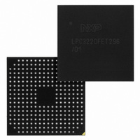
LPC3220FET296/01,5 NXP Semiconductors, LPC3220FET296/01,5 Datasheet - Page 5

LPC3220FET296/01,5
Manufacturer Part Number
LPC3220FET296/01,5
Description
IC ARM9 MCU 128K 296-TFBGA
Manufacturer
NXP Semiconductors
Series
LPC32x0r
Specifications of LPC3220FET296/01,5
Package / Case
296-TFBGA
Core Processor
ARM9
Core Size
16/32-Bit
Speed
266MHz
Connectivity
EBI/EMI, I²C, IrDA, Microwire, SPI, SSI, SSP, UART/USART, USB OTG
Peripherals
DMA, I²S, Motor Control PWM, PWM, WDT
Number Of I /o
51
Program Memory Type
ROMless
Ram Size
128K x 8
Voltage - Supply (vcc/vdd)
0.9 V ~ 3.6 V
Data Converters
A/D 3x10b
Oscillator Type
Internal
Operating Temperature
-40°C ~ 85°C
Processor Series
LPC32
Core
ARM926EJ-S
Data Bus Width
32 bit
Data Ram Size
128 KB
Interface Type
EMC
Maximum Clock Frequency
266 MHz
Number Of Timers
6
Operating Supply Voltage
1.31 V to 1.39 V
Maximum Operating Temperature
+ 85 C
Mounting Style
SMD/SMT
3rd Party Development Tools
MDK-ARM, RL-ARM, ULINK2
Minimum Operating Temperature
- 40 C
On-chip Adc
10 bit, 3 Channel
Lead Free Status / RoHS Status
Lead free / RoHS Compliant
Eeprom Size
-
Program Memory Size
-
Lead Free Status / Rohs Status
Lead free / RoHS Compliant
Other names
568-4965
935290763551
935290763551
Available stocks
Company
Part Number
Manufacturer
Quantity
Price
Company:
Part Number:
LPC3220FET296/01,5
Manufacturer:
NXP Semiconductors
Quantity:
10 000
NXP Semiconductors
ES_LPC3220
Errata sheet
Fig 2.
Scope shot 2 - actual read timing
DMA register values used in
Results of this behavior:
1. DMA reads from an external memory will have lower performance than a software
2. Potential unintended consequence when the last DMA read accesses the address
DMACConfig = 0x01
DMACCxSrcAddr = 0xe0000000; EMC_CS0
DMACCxDestAddr = 0xe0000040; EMC_CS0
DMACCxLLI = 0x0
DMACCxControl = 0x0c480004; Dest & Src addrs increment, Dest & Src 32-bit; Dburst
& Sburst size 1; transfer size 4
DMACCxConfig = 0x01
EMCStaticConfig0 = 0x00000082; 32-bit width, Byte lane state 1
read loop. The source read burst of two, to get one transfer, will significantly increase
the time to complete all transfers in the memory-to-memory DMA, therefore
decreasing the overall throughput possible on the EMC_CSx_N static memory
interface.
beyond the DMA source buffer address in the FPGA or external peripheral chip. This
extra address is the second access during the last DMA source read.
All information provided in this document is subject to legal disclaimers.
Rev. 8 — 1 February 2011
Figure
2:
ES_LPC3220
Errata sheet LPC3220
© NXP B.V. 2011. All rights reserved.
5 of 16


