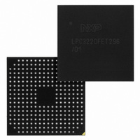
LPC3220FET296/01,5 NXP Semiconductors, LPC3220FET296/01,5 Datasheet - Page 11

LPC3220FET296/01,5
Manufacturer Part Number
LPC3220FET296/01,5
Description
IC ARM9 MCU 128K 296-TFBGA
Manufacturer
NXP Semiconductors
Series
LPC32x0r
Specifications of LPC3220FET296/01,5
Package / Case
296-TFBGA
Core Processor
ARM9
Core Size
16/32-Bit
Speed
266MHz
Connectivity
EBI/EMI, I²C, IrDA, Microwire, SPI, SSI, SSP, UART/USART, USB OTG
Peripherals
DMA, I²S, Motor Control PWM, PWM, WDT
Number Of I /o
51
Program Memory Type
ROMless
Ram Size
128K x 8
Voltage - Supply (vcc/vdd)
0.9 V ~ 3.6 V
Data Converters
A/D 3x10b
Oscillator Type
Internal
Operating Temperature
-40°C ~ 85°C
Processor Series
LPC32
Core
ARM926EJ-S
Data Bus Width
32 bit
Data Ram Size
128 KB
Interface Type
EMC
Maximum Clock Frequency
266 MHz
Number Of Timers
6
Operating Supply Voltage
1.31 V to 1.39 V
Maximum Operating Temperature
+ 85 C
Mounting Style
SMD/SMT
3rd Party Development Tools
MDK-ARM, RL-ARM, ULINK2
Minimum Operating Temperature
- 40 C
On-chip Adc
10 bit, 3 Channel
Lead Free Status / RoHS Status
Lead free / RoHS Compliant
Eeprom Size
-
Program Memory Size
-
Lead Free Status / Rohs Status
Lead free / RoHS Compliant
Other names
568-4965
935290763551
935290763551
Available stocks
Company
Part Number
Manufacturer
Quantity
Price
Company:
Part Number:
LPC3220FET296/01,5
Manufacturer:
NXP Semiconductors
Quantity:
10 000
NXP Semiconductors
ES_LPC3220
Errata sheet
3.5 RTC.1: An RTC match doesn’t drive the ONSW pin active (HIGH)
3.6 INT.1: GPI_08 does not generate an interrupt signal
Introduction:
An ONSW output pin (M15) is included in the LPC3220 to assist in waking up the chip
after power is removed from all functions except the RTC and Battery RAM. When there is
an active match condition the RTC will drive the ONSW pin HIGH. The RTC only drives
the ONSW pin while the match is active, and after 1 second of active match, if the
software has not accessed the RTC block, the ONSW pin will go low when the match is no
longer active.
Problem:
When power is removed from all functions except the RTC and Battery RAM, the RTC
does NOT drive the ONSW pin HIGH when there is an active match condition.
Work-around:
There is no work-around for this problem.
Introduction:
The LPC3220 contains 12 pins (GPI_00 - GPI_09, GPI_19, GPI_28) that function as
dedicated General Purpose Inputs. Each of these pins can generate an individual interrupt
for the input pin. Sub Interrupt Controller Register 1 (SIC1_ER) and Sub Interrupt
Controller Register 2 (SIC2_ER) contains bits that allow enabling or disabling the interrupt
for the associated pin.
Problem:
When bit nine is set to one in the Sub Interrupt Controller 2 Enable register (SIC2_ER[9])
it does not enable the interrupt for the GPI_08 pin. All other General Purpose Input pins
(GPI_00 - GPI_07, GPI_09, GPI_19, GPI_28) interrupts work correctly.
Work-around:
There is no work-around for this problem.
All information provided in this document is subject to legal disclaimers.
Rev. 8 — 1 February 2011
ES_LPC3220
Errata sheet LPC3220
© NXP B.V. 2011. All rights reserved.
11 of 16


