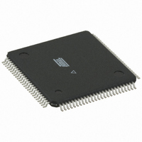
ATMEGA3290PV-10AU Atmel, ATMEGA3290PV-10AU Datasheet - Page 253

ATMEGA3290PV-10AU
Manufacturer Part Number
ATMEGA3290PV-10AU
Description
IC MCU 32K 4X40 LCD CTRL 100TQFP
Manufacturer
Atmel
Series
AVR® ATmegar
Specifications of ATMEGA3290PV-10AU
Core Processor
AVR
Core Size
8-Bit
Speed
10MHz
Connectivity
SPI, UART/USART, USI
Peripherals
Brown-out Detect/Reset, LCD, POR, PWM, WDT
Number Of I /o
69
Program Memory Size
32KB (16K x 16)
Program Memory Type
FLASH
Eeprom Size
1K x 8
Ram Size
2K x 8
Voltage - Supply (vcc/vdd)
1.8 V ~ 5.5 V
Data Converters
A/D 8x10b
Oscillator Type
Internal
Operating Temperature
-40°C ~ 85°C
Package / Case
100-TQFP, 100-VQFP
Processor Series
ATMEGA32x
Core
AVR8
Data Bus Width
8 bit
Data Ram Size
2 KB
Interface Type
SPI, USART, USI
Maximum Clock Frequency
10 MHz
Number Of Programmable I/os
69
Number Of Timers
3
Maximum Operating Temperature
+ 85 C
Mounting Style
SMD/SMT
Minimum Operating Temperature
- 40 C
On-chip Adc
10 bit, 8 Channel
For Use With
ATSTK600-TQFP100 - STK600 SOCKET/ADAPTER 100-TQFP770-1007 - ISP 4PORT ATMEL AVR MCU SPI/JTAG770-1005 - ISP 4PORT FOR ATMEL AVR MCU JTAG770-1004 - ISP 4PORT FOR ATMEL AVR MCU SPIATAVRISP2 - PROGRAMMER AVR IN SYSTEMATSTK504 - STARTER KIT AVR EXP MOD 100P LCDATJTAGICE2 - AVR ON-CHIP D-BUG SYSTEM
Lead Free Status / RoHS Status
Lead free / RoHS Compliant
Other names
ATMEGA3290PV-8AU
ATMEGA3290PV-8AU
ATMEGA3290PV-8AU
Available stocks
Company
Part Number
Manufacturer
Quantity
Price
Company:
Part Number:
ATMEGA3290PV-10AU
Manufacturer:
SIPEX
Quantity:
17 600
Part Number:
ATMEGA3290PV-10AU
Manufacturer:
ATMEL/爱特梅尔
Quantity:
20 000
- Current page: 253 of 427
- Download datasheet (9Mb)
24.9
24.10 Register Description
24.10.1
8021G–AVR–03/11
Bibliography
OCDR – On-chip Debug Register
The JTAG programming capability supports:
• Flash programming and verifying.
• EEPROM programming and verifying.
• Fuse programming and verifying.
• Lock bit programming and verifying.
The Lock bit security is exactly as in parallel programming mode. If the Lock bits LB1 or LB2 are
programmed, the OCDEN Fuse cannot be programmed unless first doing a chip erase. This is a
security feature that ensures no back-door exists for reading out the content of a secured
device.
The details on programming through the JTAG interface and programming specific JTAG
instructions are given in the section
For more information about general Boundary-scan, the following literature can be consulted:
• IEEE: IEEE Std. 1149.1-1990. IEEE Standard Test Access Port and Boundary-scan
Colin Maunder: The Board Designers Guide to Testable Logic Circuits, Addison-Wesley, 1992.
The OCDR Register provides a communication channel from the running program in the micro-
controller to the debugger. The CPU can transfer a byte to the debugger by writing to this
location. At the same time, an internal flag; I/O Debug Register Dirty – IDRD – is set to indicate
to the debugger that the register has been written. When the CPU reads the OCDR Register the
7 LSB will be from the OCDR Register, while the MSB is the IDRD bit. The debugger clears the
IDRD bit when it has read the information.
In some AVR devices, this register is shared with a standard I/O location. In this case, the OCDR
Register can only be accessed if the OCDEN Fuse is programmed, and the debugger enables
access to the OCDR Register. In all other cases, the standard I/O location is accessed.
Refer to the debugger documentation for further information on how to use this register.
Bit
0x31 (0x51)
Read/Write
Initial Value
Architecture, IEEE, 1993.
MSB/IDRD
R/W
7
0
R/W
6
0
”Programming via the JTAG Interface” on page
R/W
5
0
R/W
4
0
R/W
3
0
ATmega329P/3290P
R/W
0
2
R/W
1
0
LSB
R/W
0
0
317.
OCDR
253
Related parts for ATMEGA3290PV-10AU
Image
Part Number
Description
Manufacturer
Datasheet
Request
R

Part Number:
Description:
Manufacturer:
Atmel Corporation
Datasheet:

Part Number:
Description:
IC AVR MCU 32K 16MHZ 100TQFP
Manufacturer:
Atmel
Datasheet:

Part Number:
Description:
IC AVR MCU 32K 16MHZ 100TQFP
Manufacturer:
Atmel
Datasheet:

Part Number:
Description:
MCU AVR 32K FLASH 16MHZ 64TQFP
Manufacturer:
Atmel
Datasheet:

Part Number:
Description:
Atmega3290 Avr 8-bit Microcontroller With In-system Programmable Flash
Manufacturer:
ATMEL Corporation
Datasheet:

Part Number:
Description:
Manufacturer:
Atmel Corporation
Datasheet:

Part Number:
Description:
IC AVR MCU 32K 16MHZ 64TQFP
Manufacturer:
Atmel
Datasheet:

Part Number:
Description:
IC AVR MCU 32K 16MHZ 64-QFN
Manufacturer:
Atmel
Datasheet:

Part Number:
Description:
IC AVR MCU 32K 16MHZ 64TQFP
Manufacturer:
Atmel
Datasheet:

Part Number:
Description:
IC AVR MCU 32K 16MHZ 64-QFN
Manufacturer:
Atmel
Datasheet:

Part Number:
Description:
MCU AVR 32K FLASH 16MHZ 64TQFP
Manufacturer:
Atmel
Datasheet:

Part Number:
Description:
MCU AVR 32K FLASH 16MHZ 64QFN
Manufacturer:
Atmel
Datasheet:

Part Number:
Description:
DEV KIT FOR AVR/AVR32
Manufacturer:
Atmel
Datasheet:

Part Number:
Description:
INTERVAL AND WIPE/WASH WIPER CONTROL IC WITH DELAY
Manufacturer:
ATMEL Corporation
Datasheet:


