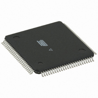
ATMEGA3290PV-10AU Atmel, ATMEGA3290PV-10AU Datasheet - Page 22

ATMEGA3290PV-10AU
Manufacturer Part Number
ATMEGA3290PV-10AU
Description
IC MCU 32K 4X40 LCD CTRL 100TQFP
Manufacturer
Atmel
Series
AVR® ATmegar
Specifications of ATMEGA3290PV-10AU
Core Processor
AVR
Core Size
8-Bit
Speed
10MHz
Connectivity
SPI, UART/USART, USI
Peripherals
Brown-out Detect/Reset, LCD, POR, PWM, WDT
Number Of I /o
69
Program Memory Size
32KB (16K x 16)
Program Memory Type
FLASH
Eeprom Size
1K x 8
Ram Size
2K x 8
Voltage - Supply (vcc/vdd)
1.8 V ~ 5.5 V
Data Converters
A/D 8x10b
Oscillator Type
Internal
Operating Temperature
-40°C ~ 85°C
Package / Case
100-TQFP, 100-VQFP
Processor Series
ATMEGA32x
Core
AVR8
Data Bus Width
8 bit
Data Ram Size
2 KB
Interface Type
SPI, USART, USI
Maximum Clock Frequency
10 MHz
Number Of Programmable I/os
69
Number Of Timers
3
Maximum Operating Temperature
+ 85 C
Mounting Style
SMD/SMT
Minimum Operating Temperature
- 40 C
On-chip Adc
10 bit, 8 Channel
For Use With
ATSTK600-TQFP100 - STK600 SOCKET/ADAPTER 100-TQFP770-1007 - ISP 4PORT ATMEL AVR MCU SPI/JTAG770-1005 - ISP 4PORT FOR ATMEL AVR MCU JTAG770-1004 - ISP 4PORT FOR ATMEL AVR MCU SPIATAVRISP2 - PROGRAMMER AVR IN SYSTEMATSTK504 - STARTER KIT AVR EXP MOD 100P LCDATJTAGICE2 - AVR ON-CHIP D-BUG SYSTEM
Lead Free Status / RoHS Status
Lead free / RoHS Compliant
Other names
ATMEGA3290PV-8AU
ATMEGA3290PV-8AU
ATMEGA3290PV-8AU
Available stocks
Company
Part Number
Manufacturer
Quantity
Price
Company:
Part Number:
ATMEGA3290PV-10AU
Manufacturer:
SIPEX
Quantity:
17 600
Part Number:
ATMEGA3290PV-10AU
Manufacturer:
ATMEL/爱特梅尔
Quantity:
20 000
- Current page: 22 of 427
- Download datasheet (9Mb)
7.6
7.6.1
7.6.2
7.6.3
8021G–AVR–03/11
Register Description
EEPROM Read/Write Access
EEARH and EEARL – EEPROM Address Register ATmega329P/3290P
EEDR – EEPROM Data Register
The EEPROM Access Registers are accessible in the I/O space.
The write access time for the EEPROM is given in
lets the user software detect when the next byte can be written. If the user code contains instruc-
tions that write the EEPROM, some precautions must be taken. In heavily filtered power
supplies, V
period of time to run at a voltage lower than specified as minimum for the clock frequency used.
See Section “7.4.2” on page 20.
In order to prevent unintentional EEPROM writes, a specific write procedure must be followed.
Refer to the description of the EEPROM Control Register for details on this.
When the EEPROM is read, the CPU is halted for four clock cycles before the next instruction is
executed. When the EEPROM is written, the CPU is halted for two clock cycles before the next
instruction is executed.
• Bits 15:10 – Reserved
These bits are reserved and will always read as zero.
• Bits 9:0 – EEAR[9:0]: EEPROM Address
The EEPROM Address Registers – EEARH and EEARL specify the EEPROM address in the
1byte EEPROM space. The EEPROM data bytes are addressed linearly between 0 and 1023.
The initial value of EEAR is undefined. A proper value must be written before the EEPROM may
be accessed.
• Bits 7:0 – EEDR7:0: EEPROM Data
For the EEPROM write operation, the EEDR Register contains the data to be written to the
EEPROM in the address given by the EEAR Register. For the EEPROM read operation, the
EEDR contains the data read out from the EEPROM at the address given by EEAR.
Bit
0x22 (0x42)
0x21 (0x41)
Read/Write
Initial Value
Bit
0x20 (0x40)
Read/Write
Initial Value
CC
EEAR7
R/W
is likely to rise or fall slowly on power-up/down. This causes the device for some
15
MSB
R
0
X
R/W
–
7
7
0
EEAR6
R/W
14
R
X
–
6
0
R/W
6
0
EEAR5
R/W
13
R
X
–
5
0
for details on how to avoid problems in these situations.
R/W
5
0
EEAR4
R/W
12
R
–
4
0
X
R/W
4
0
EEAR3
R/W
11
R
X
–
3
0
Table
R/W
3
0
EEAR2
R/W
R/W
ATmega329P/3290P
10
X
X
–
2
7-1. A self-timing function, however,
R/W
2
0
EEAR9
EEAR1
R/W
R/W
X
9
1
X
R/W
1
0
EEAR8
EEAR0
R/W
R/W
8
0
X
X
LSB
R/W
EEARH
EEARL
0
0
EEDR
22
Related parts for ATMEGA3290PV-10AU
Image
Part Number
Description
Manufacturer
Datasheet
Request
R

Part Number:
Description:
Manufacturer:
Atmel Corporation
Datasheet:

Part Number:
Description:
IC AVR MCU 32K 16MHZ 100TQFP
Manufacturer:
Atmel
Datasheet:

Part Number:
Description:
IC AVR MCU 32K 16MHZ 100TQFP
Manufacturer:
Atmel
Datasheet:

Part Number:
Description:
MCU AVR 32K FLASH 16MHZ 64TQFP
Manufacturer:
Atmel
Datasheet:

Part Number:
Description:
Atmega3290 Avr 8-bit Microcontroller With In-system Programmable Flash
Manufacturer:
ATMEL Corporation
Datasheet:

Part Number:
Description:
Manufacturer:
Atmel Corporation
Datasheet:

Part Number:
Description:
IC AVR MCU 32K 16MHZ 64TQFP
Manufacturer:
Atmel
Datasheet:

Part Number:
Description:
IC AVR MCU 32K 16MHZ 64-QFN
Manufacturer:
Atmel
Datasheet:

Part Number:
Description:
IC AVR MCU 32K 16MHZ 64TQFP
Manufacturer:
Atmel
Datasheet:

Part Number:
Description:
IC AVR MCU 32K 16MHZ 64-QFN
Manufacturer:
Atmel
Datasheet:

Part Number:
Description:
MCU AVR 32K FLASH 16MHZ 64TQFP
Manufacturer:
Atmel
Datasheet:

Part Number:
Description:
MCU AVR 32K FLASH 16MHZ 64QFN
Manufacturer:
Atmel
Datasheet:

Part Number:
Description:
DEV KIT FOR AVR/AVR32
Manufacturer:
Atmel
Datasheet:

Part Number:
Description:
INTERVAL AND WIPE/WASH WIPER CONTROL IC WITH DELAY
Manufacturer:
ATMEL Corporation
Datasheet:


