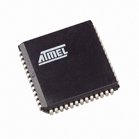
AT89C5131A-S3SUM Atmel, AT89C5131A-S3SUM Datasheet - Page 96

AT89C5131A-S3SUM
Manufacturer Part Number
AT89C5131A-S3SUM
Description
IC 8051 MCU FLASH 32K USB 52PLCC
Manufacturer
Atmel
Series
AT89C513xr
Datasheet
1.AT89C5130A-PUTUM.pdf
(188 pages)
Specifications of AT89C5131A-S3SUM
Core Processor
C52X2
Core Size
8-Bit
Speed
48MHz
Connectivity
I²C, SPI, UART/USART, USB
Peripherals
LED, POR, PWM, WDT
Number Of I /o
34
Program Memory Size
32KB (32K x 8)
Program Memory Type
FLASH
Eeprom Size
4K x 8
Ram Size
1.25K x 8
Voltage - Supply (vcc/vdd)
2.7 V ~ 5.5 V
Oscillator Type
Internal
Operating Temperature
-40°C ~ 85°C
Package / Case
52-PLCC
Processor Series
AT89x
Core
8051
Data Bus Width
8 bit
Data Ram Size
1.25 KB
Interface Type
2-Wire, EUART, SPI, USB
Maximum Clock Frequency
48 MHz
Number Of Programmable I/os
34
Number Of Timers
16 bit
Operating Supply Voltage
2.7 V to 5.5 V
Maximum Operating Temperature
+ 85 C
Mounting Style
SMD/SMT
3rd Party Development Tools
PK51, CA51, A51, ULINK2
Development Tools By Supplier
AT89STK-05
Minimum Operating Temperature
- 40 C
Package
52PLCC
Device Core
8051
Family Name
89C
Maximum Speed
48 MHz
For Use With
AT89OCD-01 - USB EMULATOR FOR AT8XC51 MCUAT89STK-10 - KIT EVAL APPL MASS STORAGEAT89STK-05 - KIT STARTER FOR AT89C5131
Lead Free Status / RoHS Status
Lead free / RoHS Compliant
Data Converters
-
Lead Free Status / Rohs Status
Details
Available stocks
Company
Part Number
Manufacturer
Quantity
Price
Company:
Part Number:
AT89C5131A-S3SUM
Manufacturer:
ATMEL
Quantity:
46
19.3.1.1
19.3.1.2
19.3.2
96
AT89C5130A/31A-M
Transmission Formats
Master Mode
Slave Mode
When the Master device transmits data to the Slave device via the MOSI line, the Slave device
responds by sending data to the Master device via the MISO line. This implies full-duplex trans-
mission with both data out and data in synchronized with the same clock (Figure 19-3).
Figure 19-3. Full-duplex Master/Slave Interconnection
The SPI operates in Master mode when the Master bit, MSTR
Only one Master SPI device can initiate transmissions. Software begins the transmission from a
Master SPI module by writing to the Serial Peripheral Data Register (SPDAT). If the shift register
is empty, the byte is immediately transferred to the shift register. The byte begins shifting out on
MOSI pin under the control of the serial clock, SCK. Simultaneously, another byte shifts in from
the Slave on the Master’s MISO pin. The transmission ends when the Serial Peripheral transfer
data flag, SPIF, in SPSTA becomes set. At the same time that SPIF becomes set, the received
byte from the Slave is transferred to the receive data register in SPDAT. Software clears SPIF
by reading the Serial Peripheral Status register (SPSTA) with the SPIF bit set, and then reading
the SPDAT.
The SPI operates in Slave mode when the Master bit, MSTR
cleared. Before a data transmission occurs, the Slave Select pin, SS, of the Slave device must
be set to’0’. SS must remain low until the transmission is complete.
In a Slave SPI module, data enters the shift register under the control of the SCK from the Mas-
ter SPI module. After a byte enters the shift register, it is immediately transferred to the receive
data register in SPDAT, and the SPIF bit is set. To prevent an overflow condition, Slave software
must then read the SPDAT before another byte enters the shift register
complete the write to the SPDAT (shift register) at least one bus cycle before the Master SPI
starts a transmission. If the write to the data register is late, the SPI transmits the data already in
the shift register from the previous transmission.
Software can select any of four combinations of serial clock (SCK) phase and polarity using two
bits in the SPCON: the Clock POLarity (CPOL
the default SCK line level in idle state. It has no significant effect on the transmission format.
CPHA defines the edges on which the input data are sampled and the edges on which the
1.
2.
3.
4.
The SPI module should be configured as a Master before it is enabled (SPEN set). Also the Mas-
The SPI module should be configured as a Slave before it is enabled (SPEN set).
The maximum frequency of the SCK for an SPI configured as a Slave is
Before writing to the CPOL and CPHA bits, the SPI should be disabled (SPEN =’0’).
ter SPI should be configured before the Slave SPI.
Clock Generator
SPI
Master MCU
8-bit Shift Register
MOSI
SCK
SS
MISO
VDD
(4)
) and the Clock PHAse (CPHA
MOSI
MISO
SCK
VSS
SS
(1)
8-bit Shift Register
, in the SPCON register is set.
Slave MCU
(2)
, in the SPCON register is
F
(3)
CLK PERIPH
. A Slave SPI must
4
). CPOL defines
/2
4337K–USB–04/08
.


