AT89C5131A-S3SUM Atmel, AT89C5131A-S3SUM Datasheet - Page 18
AT89C5131A-S3SUM
Manufacturer Part Number
AT89C5131A-S3SUM
Description
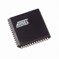
IC 8051 MCU FLASH 32K USB 52PLCC
Manufacturer
Atmel
Series
AT89C513xr
Datasheet
1.AT89C5130A-PUTUM.pdf
(188 pages)
Specifications of AT89C5131A-S3SUM
Core Processor
C52X2
Core Size
8-Bit
Speed
48MHz
Connectivity
I²C, SPI, UART/USART, USB
Peripherals
LED, POR, PWM, WDT
Number Of I /o
34
Program Memory Size
32KB (32K x 8)
Program Memory Type
FLASH
Eeprom Size
4K x 8
Ram Size
1.25K x 8
Voltage - Supply (vcc/vdd)
2.7 V ~ 5.5 V
Oscillator Type
Internal
Operating Temperature
-40°C ~ 85°C
Package / Case
52-PLCC
Processor Series
AT89x
Core
8051
Data Bus Width
8 bit
Data Ram Size
1.25 KB
Interface Type
2-Wire, EUART, SPI, USB
Maximum Clock Frequency
48 MHz
Number Of Programmable I/os
34
Number Of Timers
16 bit
Operating Supply Voltage
2.7 V to 5.5 V
Maximum Operating Temperature
+ 85 C
Mounting Style
SMD/SMT
3rd Party Development Tools
PK51, CA51, A51, ULINK2
Development Tools By Supplier
AT89STK-05
Minimum Operating Temperature
- 40 C
Package
52PLCC
Device Core
8051
Family Name
89C
Maximum Speed
48 MHz
For Use With
AT89OCD-01 - USB EMULATOR FOR AT8XC51 MCUAT89STK-10 - KIT EVAL APPL MASS STORAGEAT89STK-05 - KIT STARTER FOR AT89C5131
Lead Free Status / RoHS Status
Lead free / RoHS Compliant
Data Converters
-
Lead Free Status / Rohs Status
Details
Available stocks
Company
Part Number
Manufacturer
Quantity
Price
Company:

Part Number:
AT89C5131A-S3SUM
Manufacturer:
ATMEL
Quantity:
46


18
AT89C5130A/31A-M
Reset Value = 0000 0000b
Table 5-3.
Reset Value = 0000 0000b
Table 5-4.
Reset Value = 0000 0000b
Table 5-5.
Bit Number
Bit Number
7-1
7-3
R3
7
0
7
2
1
0
7
-
-
CKCON1 (S:AFh)
Clock Control Register 1
PLLCON (S:A3h)
PLL Control Register
PLLDIV (S:A4h)
PLL Divider Register
Mnemonic Description
Mnemonic Description
PLOCK
PLLEN
EXT48
SPIX2
Bit
Bit
R2
6
6
6
-
-
-
-
Reserved
The value read from this bit is always 0. Do not set this bit.
SPI Clock
This control bit is validated when the CPU clock X2 is set. When X2 is low,
this bit has no effect.
Clear to select 6 clock periods per peripheral clock cycle.
Set to select 12 clock periods per peripheral clock cycle.
Reserved
The value read from this bit is always 0. Do not set this bit.
External 48 MHz Enable Bit
Set this bit to bypass the PLL and disable the crystal oscillator.
Clear this bit to select the PLL output as USB clock and to enable the crystal
oscillator.
PLL Enable Bit
Set to enable the PLL.
Clear to disable the PLL.
PLL Lock Indicator
Set by hardware when PLL is locked.
Clear by hardware when PLL is unlocked.
R1
5
5
5
-
-
R0
4
4
4
-
-
N3
3
3
3
-
-
EXT48
N2
2
2
2
-
PLLEN
N1
1
1
1
-
4337K–USB–04/08
PLOCK
SPIX2
N0
0
0
0
Related parts for AT89C5131A-S3SUM
Image
Part Number
Description
Manufacturer
Datasheet
Request
R

Part Number:
Description:
Manufacturer:
Atmel Corporation
Datasheet:
Part Number:
Description:
Manufacturer:
Atmel Corporation
Datasheet:

Part Number:
Description:
IC 8051 MCU FLASH 32K USB 32QFN
Manufacturer:
Atmel
Datasheet:

Part Number:
Description:
IC MCU 32KB 3-3.6V USB 48-VQFN
Manufacturer:
Atmel
Datasheet:

Part Number:
Description:
MCU 8051 32K FLASH USB 28-SOIC
Manufacturer:
Atmel
Datasheet:

Part Number:
Description:
IC 8051 MCU FLASH 32K USB 64VQFP
Manufacturer:
Atmel
Datasheet:
Part Number:
Description:
MCU 8051 32K FLASH USB 64-VQFP
Manufacturer:
Atmel
Datasheet:
Part Number:
Description:
MCU 8051 32K FLASH USB 28-SOIC
Manufacturer:
Atmel
Datasheet:

Part Number:
Description:
MCU 8051 32K FLASH USB 52-PLCC
Manufacturer:
Atmel
Datasheet:
Part Number:
Description:
IC 8051 MCU FLASH 32K USB 48QFN
Manufacturer:
Atmel
Datasheet:
Part Number:
Description:
IC 8051 MCU FLASH 32K USB 64VQFP
Manufacturer:
Atmel
Datasheet:
Part Number:
Description:
IC 8051 MCU FLASH 32K USB 32QFN
Manufacturer:
Atmel
Datasheet:
Part Number:
Description:
IC 8051 MCU FLASH 32K USB 52PLCC
Manufacturer:
Atmel
Datasheet:
Part Number:
Description:
IC 8051 MCU FLASH 32K USB 28SOIC
Manufacturer:
Atmel
Datasheet: